
3.1 Powering the TS1800 Evaluation Base Board
The TS1800 Evaluation Base Board can be powered directly through the USB Type-C® ports (J29 and/or J24). The 5V USB input is regulated to 3.3V by the MCP1727 voltage regulator.
Alternatively, the TS1800 Evaluation Board can be powered by an external power supply connected through the +5V In pin (J25). The 5V is regulated to 3.3V, consistent with operation through the USB Type-C® port.
Shunt diodes D7 or D8 may be used to measure total system power consumption when powering the board through a USB Type-C® connection.
When the board is powered, D15 (+5V), D16 (+3.3V) and D17 (+1.8V) turn on.
The board power-up is shown in the following figure:
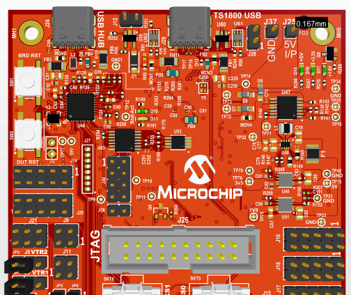
- Voltage Rails: +5V, +3.3V and +1.8V
- Test points:
- TP71: +5V
- TP76: +3.3V
- TP78: +1.8V
USB Hub (J24)
When the J24 USB-C port is connected to a PC:
- The power supply circuit generates 5V, 3.3V and 1.8V rails, which can be probed at TP75 (5V), TP76 (3.3V) and TP78 (1.8V).
- The PKOB chip monitors the 3.3V, 1.8V and Power Good signals to verify power status.
- The VBUS (5V) input must remain within the 4.5V to 5.5V range. If the voltage falls outside this range, the hub will not enumerate.
- After confirming the above conditions, the hub should enumerate successfully.
- The hub includes four downstream devices: two FT4222 devices, one MCP2221 and one PKOB device.
Please note that enumeration may require at least 20 seconds due to the presence of multiple devices.
DUT USB (J29)
This USB port is designated for the Device Under Test (TS1800 ASIC).
- Similar to the USB hub, the power supply circuit generates 5V, 3.3V and 1.8V rails, which can be probed at TP75 (5V), TP76 (3.3V) and TP78 (1.8V).
- This interface operates only when the appropriate TS1800 firmware has been programmed. If the device is blank, the connection functions solely as a power source.
- This connection is not recommended unless specifically required for TS1800 USB interface testing.
ARM Standard JTAG Connector - 20-pin, 0.10 (J26)
An external debugger accesses the chip through a standard JTAG interface. The ARM Debug Access Port supports both the 2-pin Serial Wire Debug (SWD) interface and the 4-pin JTAG interface.