
5 Edge Detection
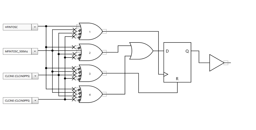
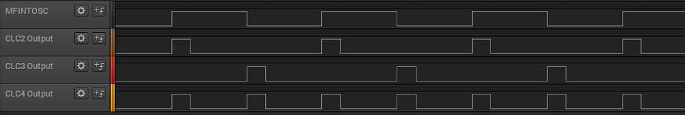
Edge detection is useful in cases when a system needs to respond to a change of state on a signal. Edge detection circuits can be implemented in hardware using the CLC module, and operate independent of the core. This allows the CPU core to tend to other important tasks, and eliminates any delays that would be involved in processing these signals using the CPU without CLC modules. This application of the CLC module can be very useful in cases where the CPU core is in Sleep mode to save power. The CLC module will remain active in Sleep, and the circuit that was configured will continue to capture the input edges as designed. The circuit implemented in this application is capable of detecting any rising or falling edge of the input signal. In this example the MFINTOSC signal is used as the input to the edge detection circuit.
Edge Detection Initialization Code
/*This code block configures the CLCs
for Edge Detection.
*/
void CLC1_Initialize(void) {
CLCSELECT = 0x00; // SLCT 0
CLCnPOL = 0x00; // Gate and CLCnOUT Output polarity Selection
CLCnSEL0 = 0x09; // D1S HFINTOSC
CLCnSEL1 = 0x0B; // D2S MFINTOSC_500khz
CLCnSEL2 = 0x00; // D3S CLCIN0 (CLCIN0PPS)
CLCnSEL3 = 0x00; // D4S CLCIN0 (CLCIN0PPS)
CLCnGLS0 = 0x02; // CLCn Gate 1 Logic Selection
CLCnGLS1 = 0x08; // CLCn Gate 2 Logic Selection
CLCnGLS2 = 0x00; // CLCn Gate 3 Logic Selection
CLCnGLS3 = 0x00; // CLCn Gate 4 Logic Selection
CLCDATA = 0x00; // CLC1OUT 0
CLCnCON = 0x85; // EN enabled; INTN disabled; INTP disabled; MODE 2-input D flip-flop with R
}
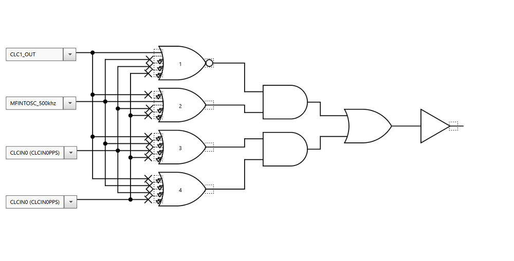
void CLC2_Initialize(void) {
CLCSELECT = 0x01; // SLCT 1
CLCnPOL = 0x01; // Gate and CLCnOUT Output polarity Selection
CLCnSEL0 = 0x33; // D1S CLC1_OUT
CLCnSEL1 = 0x0B; // D2S MFINTOSC_500khz
CLCnSEL2 = 0x00; // D3S CLCIN0 (CLCIN0PPS)
CLCnSEL3 = 0x00; // D4S CLCIN0 (CLCIN0PPS)
CLCnGLS0 = 0x02; // CLCn Gate 1 Logic Selection
CLCnGLS1 = 0x08; // CLCn Gate 2 Logic Selection
CLCnGLS2 = 0x00; // CLCn Gate 3 Logic Selection
CLCnGLS3 = 0x00; // CLCn Gate 4 Logic Selection
CLCDATA = 0x00; // CLC2OUT 0
CLCnCON = 0x80; // EN enabled; INTN disabled; INTP disabled; MODE AND-OR
}
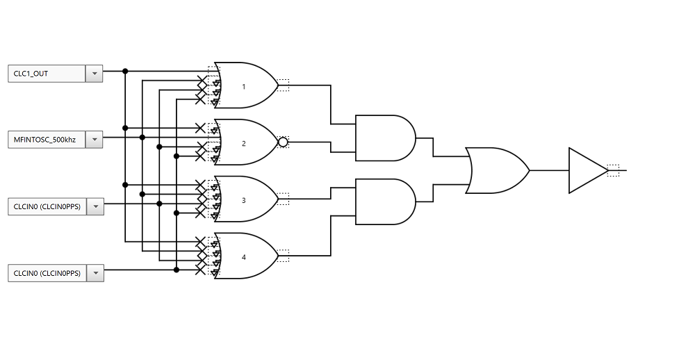
void CLC3_Initialize(void) {
CLCSELECT = 0x02; // SLCT 2
CLCnPOL = 0x02; // Gate and CLCnOUT Output polarity Selection
CLCnSEL0 = 0x33; // D1S CLC1_OUT
CLCnSEL1 = 0x0B; // D2S MFINTOSC_500khz
CLCnSEL2 = 0x00; // D3S CLCIN0 (CLCIN0PPS)
CLCnSEL3 = 0x00; // D4S CLCIN0 (CLCIN0PPS)
CLCnGLS0 = 0x02; // CLCn Gate 1 Logic Selection
CLCnGLS1 = 0x08; // CLCn Gate 2 Logic Selection
CLCnGLS2 = 0x00; // CLCn Gate 3 Logic Selection
CLCnGLS3 = 0x00; // CLCn Gate 4 Logic Selection
CLCDATA = 0x00; // CLC3OUT 0
CLCnCON = 0x80; // EN enabled; INTN disabled; INTP disabled; MODE AND-OR
}
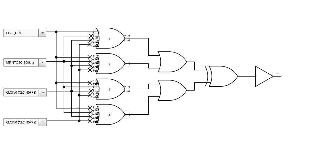
void CLC4_Initialize(void) {
CLCSELECT = 0x03; // SLCT 3
CLCnPOL = 0x00; // Gate and CLCnOUT Output polarity Selection
CLCnSEL0 = 0x33; // D1S CLC1_OUT
CLCnSEL1 = 0x0B; // D2S MFINTOSC_500khz
CLCnSEL2 = 0x00; // D3S CLCIN0 (CLCIN0PPS)
CLCnSEL3 = 0x00; // D4S CLCIN0 (CLCIN0PPS)
CLCnGLS0 = 0x02; // CLCn Gate 1 Logic Selection
CLCnGLS1 = 0x00; // CLCn Gate 2 Logic Selection
CLCnGLS2 = 0x08; // CLCn Gate 3 Logic Selection
CLCnGLS3 = 0x00; // CLCn Gate 4 Logic Selection
CLCDATA = 0x00; // CLC4OUT 0
CLCnCON = 0x81; // EN enabled; INTN disabled; INTP disabled; MODE OR-XOR
}