3 2-to-4 Binary Decoder
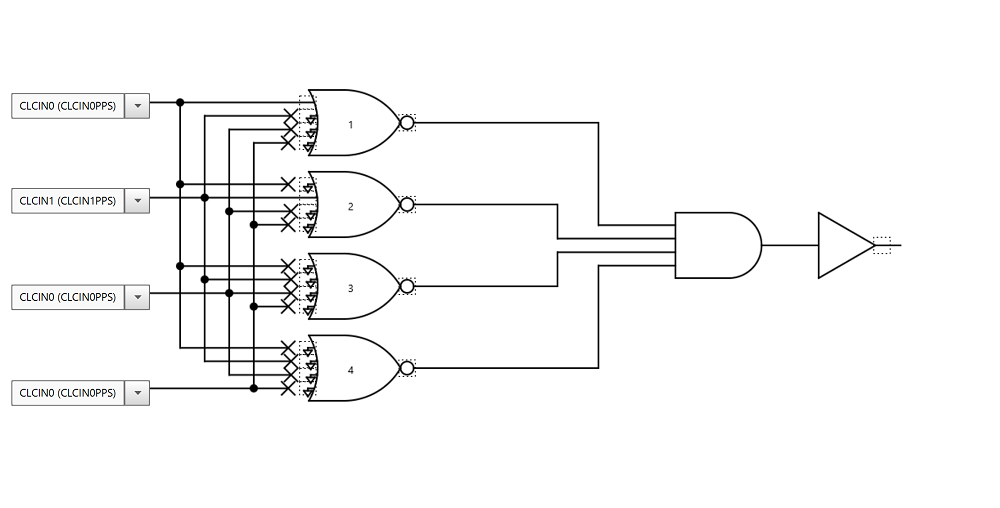
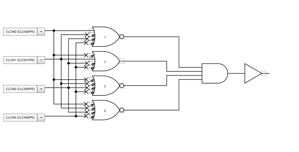
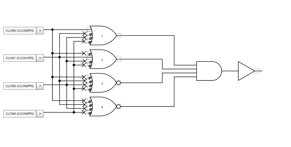
A binary decoder is a logic circuit that converts binary data from n inputs to 2n outputs. This example will demonstrate how to implement 2-to-4 binary decoder using CLCs. Table 3-1 below shows the truth table for the 3-to-8 binary decoder, and Figure 3-1 illustrates the resulting circuit that should be implemented using CLCs, based on the derived Boolean expressions. MCC was used to setup the CLC modules for this application, and the configuration settings can be found in Figure 3-2, Figure 3-3, Figure 3-4 and Figure 3-5. The configuration code can be found in 2-to-4 Binary Decoder Initialization Code.
| A1 | A0 | Y3 | Y2 | Y1 | Y0 |
|---|---|---|---|---|---|
0 | 0 | 1 | 0 | 0 | 0 |
0 | 1 | 0 | 1 | 0 | 0 |
1 | 0 | 0 | 0 | 1 | 0 |
1 | 1 | 0 | 0 | 0 | 1 |


2-to-4 Binary Decoder Initialization Code
/*This code block configures the CLCs
for 2-to-4 Binary Decoder.
  */

void CLC1_Initialize(void) {
    CLCSELECT = 0x00;	    // SLCT 0
    CLCnPOL = 0x0F;	      // Gate and CLCnOUT Output polarity Selection
    CLCnSEL0 = 0x00;	     // D1S CLCIN0 (CLCIN0PPS)
    CLCnSEL1 = 0x01;	     // D2S CLCIN1 (CLCIN1PPS)
    CLCnSEL2 = 0x00;	     // D3S CLCIN0 (CLCIN0PPS)
    CLCnSEL3 = 0x00;	     // D4S CLCIN0 (CLCIN0PPS)
    CLCnGLS0 = 0x02;	     // CLCn Gate 1 Logic Selection
    CLCnGLS1 = 0x08;	     // CLCn Gate 2 Logic Selection
    CLCnGLS2 = 0x00;	     // CLCn Gate 3 Logic Selection
    CLCnGLS3 = 0x00;	     // CLCn Gate 4 Logic Selection
    CLCDATA = 0x00;	      // CLC1OUT 0
    CLCnCON = 0x82;	      // EN enabled; INTN disabled; INTP disabled; MODE 4-input AND
}

void CLC2_Initialize(void) {
    CLCSELECT = 0x01;	    // SLCT 1
    CLCnPOL = 0x0D;	      // Gate and CLCnOUT Output polarity Selection
    CLCnSEL0 = 0x00;	     // D1S CLCIN0 (CLCIN0PPS)
    CLCnSEL1 = 0x01;	     // D2S CLCIN1 (CLCIN1PPS)
    CLCnSEL2 = 0x00;	     // D3S CLCIN0 (CLCIN0PPS)
    CLCnSEL3 = 0x00;	     // D4S CLCIN0 (CLCIN0PPS)
    CLCnGLS0 = 0x02;	     // CLCn Gate 1 Logic Selection
    CLCnGLS1 = 0x08;	     // CLCn Gate 2 Logic Selection
    CLCnGLS2 = 0x00;	     // CLCn Gate 3 Logic Selection
    CLCnGLS3 = 0x00;	     // CLCn Gate 4 Logic Selection
    CLCDATA = 0x00;	      // CLC2OUT 0
    CLCnCON = 0x82;	      // EN enabled; INTN disabled; INTP disabled; MODE 4-input AND
}

void CLC5_Initialize(void) {
    CLCSELECT = 0x04;	    // SLCT 4
    CLCnPOL = 0x0E;	      // Gate and CLCnOUT Output polarity Selection
    CLCnSEL0 = 0x00;	     // D1S CLCIN0 (CLCIN0PPS)
    CLCnSEL1 = 0x01;	     // D2S CLCIN1 (CLCIN1PPS)
    CLCnSEL2 = 0x00;	     // D3S CLCIN0 (CLCIN0PPS)
    CLCnSEL3 = 0x00;	     // D4S CLCIN0 (CLCIN0PPS)
    CLCnGLS0 = 0x02;	     // CLCn Gate 1 Logic Selection
    CLCnGLS1 = 0x08;	     // CLCn Gate 2 Logic Selection
    CLCnGLS2 = 0x00;	     // CLCn Gate 3 Logic Selection
    CLCnGLS3 = 0x00;	     // CLCn Gate 4 Logic Selection
    CLCDATA = 0x00;	      // CLC5OUT 0
    CLCnCON = 0x82;	      // EN enabled; INTN disabled; INTP disabled; MODE 4-input AND
}

void CLC6_Initialize(void) {
    CLCSELECT = 0x05;	    // SLCT 5
    CLCnPOL = 0x0C;	      // Gate and CLCnOUT Output polarity Selection
    CLCnSEL0 = 0x00;	     // D1S CLCIN0 (CLCIN0PPS)
    CLCnSEL1 = 0x01;	     // D2S CLCIN1 (CLCIN1PPS)
    CLCnSEL2 = 0x00;	     // D3S CLCIN0 (CLCIN0PPS)
    CLCnSEL3 = 0x00;	     // D4S CLCIN0 (CLCIN0PPS)
    CLCnGLS0 = 0x02;	     // CLCn Gate 1 Logic Selection
    CLCnGLS1 = 0x08;	     // CLCn Gate 2 Logic Selection
    CLCnGLS2 = 0x00;	     // CLCn Gate 3 Logic Selection
    CLCnGLS3 = 0x00;	     // CLCn Gate 4 Logic Selection
    CLCDATA = 0x00;	      // CLC6OUT 0
    CLCnCON = 0x82;	      // EN enabled; INTN disabled; INTP disabled; MODE 4-input AND
}