2 8-to-3 Binary Encoder
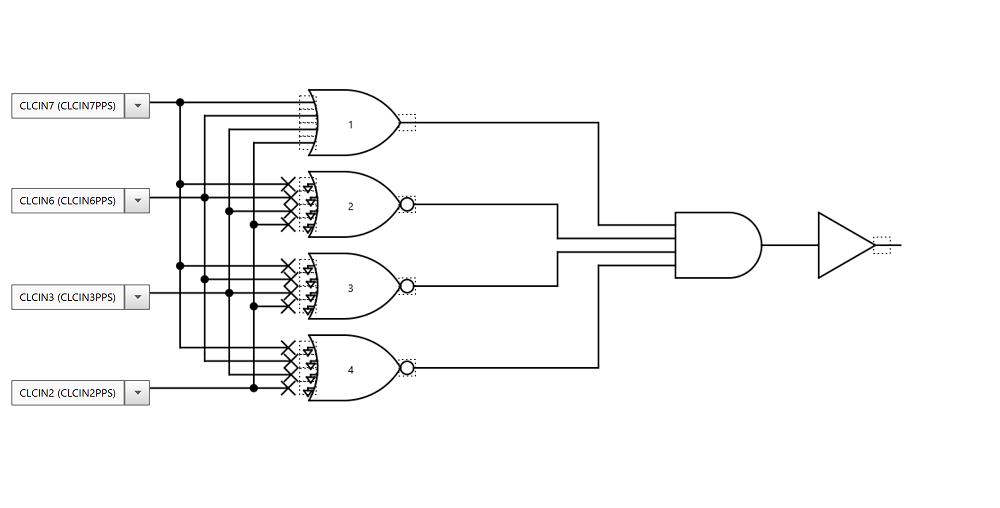
In the previous example, two CLCs were used to implement a 4-to-2 binary encoder in hardware. The following example will demonstrate how the same principals can be applied to implement an 8-to-3 binary encoder using the PIC18F47Q43 and three CLCs. Table 2-1 below shows the truth table for the 8-to-3 binary encoder, and Figure 2-1 illustrates the resulting circuit that should be implemented using CLCs based on the derived Boolean expressions. The Boolean expressions derived from the truth table show that the 8-to-3 binary encoder can be implemented using three OR gates, each of which will be implemented using a CLC. The eight input signals in this example were configured using PPS as the CLC inputs to each OR gate based on the Boolean expressions below. The three CLC output signals, which represent the 3-bit encoded binary output, were also configured using PPS and are tied to pins RA6, RA5, and RA4. MCC was used to setup the CLCs for the 8-to-3 binary encoder, and the configurations for each CLC are illustrated in Figure 2-2, Figure 2-3 and Figure 2-4, respectively.
| Y7 | Y6 | Y5 | Y4 | Y3 | Y2 | Y1 | Y0 | A2 | A1 | A0 |
|---|---|---|---|---|---|---|---|---|---|---|
0 | 0 | 0 | 0 | 0 | 0 | 0 | 1 | 0 | 0 | 0 |
0 | 0 | 0 | 0 | 0 | 0 | 1 | 0 | 0 | 0 | 1 |
0 | 0 | 0 | 0 | 0 | 1 | 0 | 0 | 0 | 1 | 0 |
0 | 0 | 0 | 0 | 1 | 0 | 0 | 0 | 0 | 1 | 1 |
0 | 0 | 0 | 1 | 0 | 0 | 0 | 0 | 1 | 0 | 0 |
0 | 0 | 1 | 0 | 0 | 0 | 0 | 0 | 1 | 0 | 1 |
0 | 1 | 0 | 0 | 0 | 0 | 0 | 0 | 1 | 1 | 0 |
1 | 0 | 0 | 0 | 0 | 0 | 0 | 0 | 1 | 1 | 1 |


8-to-3 Binary Encoder Initialization Code
/*This code block configures the CLCs
for 8-to-3 Binary Encoder.
  */

void CLC1_Initialize(void) {
    CLCSELECT = 0x00;	    // SLCT 0
    CLCnPOL = 0x0E;	      // Gate and CLCnOUT Output polarity Selection
    CLCnSEL0 = 0x07;	     // D1S CLCIN7 (CLCIN7PPS)
    CLCnSEL1 = 0x05;	     // D2S CLCIN5 (CLCIN5PPS)
    CLCnSEL2 = 0x03;	     // D3S CLCIN3 (CLCIN3PPS)
    CLCnSEL3 = 0x01;	     // D4S CLCIN1 (CLCIN1PPS)
    CLCnGLS0 = 0xAA;	     // CLCn Gate 1 Logic Selection
    CLCnGLS1 = 0x00;	     // CLCn Gate 2 Logic Selection
    CLCnGLS2 = 0x00;	     // CLCn Gate 3 Logic Selection
    CLCnGLS3 = 0x00;	     // CLCn Gate 4 Logic Selection
    CLCDATA = 0x00;	      // CLC1OUT 0
    CLCnCON = 0x82;	      // EN enabled; INTN disabled; INTP disabled; MODE 4-input AND
}

void CLC2_Initialize(void) {
    CLCSELECT = 0x01;	    // SLCT 1;
    CLCnPOL = 0x0E;	      // Gate and CLCnOUT Output polarity Selection
    CLCnSEL0 = 0x07;	     // D1S CLCIN7 (CLCIN7PPS);
    CLCnSEL1 = 0x06;	     // D2S CLCIN6 (CLCIN6PPS);
    CLCnSEL2 = 0x03;	     // D3S CLCIN3 (CLCIN3PPS);
    CLCnSEL3 = 0x02;	     // D4S CLCIN2 (CLCIN2PPS);
    CLCnGLS0 = 0xAA;	     // CLCn Gate 1 Logic Selection
    CLCnGLS1 = 0x00;	     // CLCn Gate 2 Logic Selection
    CLCnGLS2 = 0x00;	     // CLCn Gate 3 Logic Selection
    CLCnGLS3 = 0x00;	     // CLCn Gate 4 Logic Selection
    CLCDATA = 0x00;	      // CLC2OUT 0
    CLCnCON = 0x82;	      // EN enabled; INTN disabled; INTP disabled; MODE 4-input AND
}

void CLC5_Initialize(void) {
    CLCSELECT = 0x04;	    // SLCT 4
    CLCnPOL = 0x0E;	      // Gate and CLCnOUT Output polarity Selection
    CLCnSEL0 = 0x07;	     // D1S CLCIN7 (CLCIN7PPS)
    CLCnSEL1 = 0x06;	     // D2S CLCIN6 (CLCIN6PPS)
    CLCnSEL2 = 0x05;	     // D3S CLCIN5 (CLCIN5PPS)
    CLCnSEL3 = 0x04;	     // D4S CLCIN4 (CLCIN4PPS)
    CLCnGLS0 = 0xAA;	     // CLCn Gate 1 Logic Selection
    CLCnGLS1 = 0x00;	     // CLCn Gate 2 Logic Selection
    CLCnGLS2 = 0x00;	     // CLCn Gate 3 Logic Selection
    CLCnGLS3 = 0x00;	     // CLCn Gate 4 Logic Selection
    CLCDATA = 0x00;	      // CLC5OUT 0
    CLCnCON = 0x82;	      // EN enabled; INTN disabled; INTP disabled; MODE 4-input AND
}