1 4-to-2 Binary Encoder
Binary encoders allow users to take multiple digital inputs (2n input bits) at one time and convert them into a single-encoded binary output (n output bits) using combinational logic. This can be useful in applications where there are several inputs that need to be monitored at the same time for changes, as the binary encoder circuit creates a shortened binary string that is representative of the logic state on each individual input signal. PIC® microcontroller devices equipped with the Configurable Logic Cell (CLC) module can be used to implement a binary encoder circuit using only CLCs, without the need for any additional hardware. The following example will demonstrate how two CLCs can be used to implement a 4-to-2 binary encoder in hardware using the PIC18F47Q43.
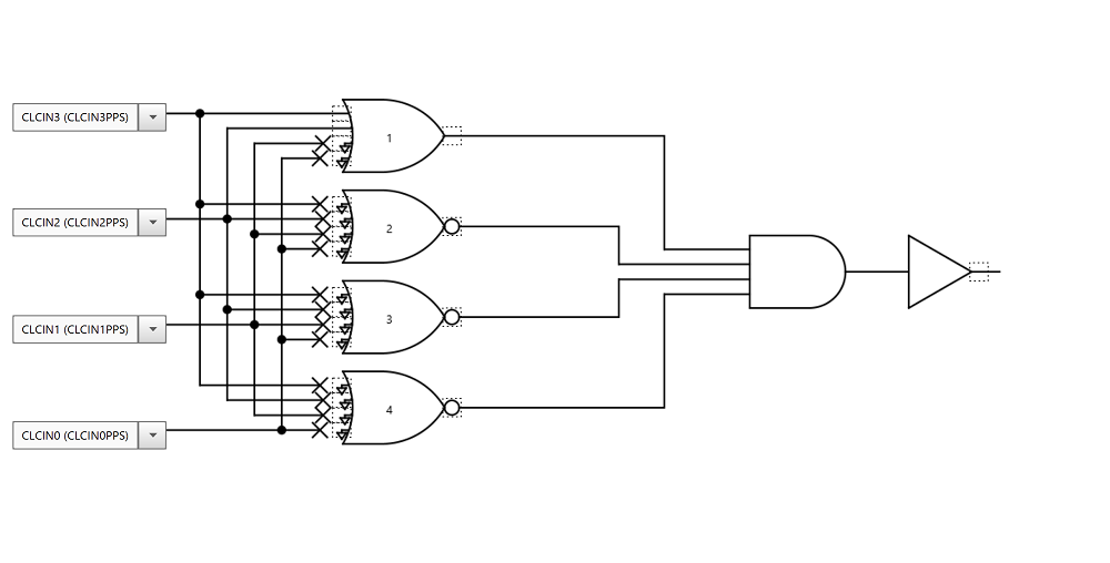
Table 1-1 contains the truth table as well as the corresponding Boolean expressions that were used to create the circuit needed for the 4-to-2 binary encoder. The resulting Boolean expressions show that the binary encoder can be implemented using two OR gates, in which the OR gate outputs provide the 2-bit binary encoded output string (the resulting circuit is illustrated by Figure 1-1). The four input signals, which in this example were standard GPIO pins, were configured using Peripheral Pin Select (PPS) as the CLC inputs to each OR gate based on the Boolean expressions below. The two CLC output signals, which are representative of the 2-bit encoded binary output, were also configured using PPS and are represented by the LEDs tied to pins RA5 and RA4. The MPLAB® Code Configurator (MCC) tool was used to setup the CLCs for this example, and the configurations for CLC1 and CLC2 are illustrated in Figure 1-2 and Figure 1-3, respectively.
| Y3 | Y2 | Y1 | Y0 | A1 | A0 |
|---|---|---|---|---|---|
0 | 0 | 0 | 1 | 0 | 0 |
0 | 0 | 1 | 0 | 0 | 1 |
0 | 1 | 0 | 0 | 1 | 0 |
1 | 0 | 0 | 0 | 1 | 1 |


4-to-2 Binary Encoder Initialization Code
/*This code block configures the CLCs
for 4-to-2 Binary Encoder.
  */

void CLC1_Initialize(void) {
    CLCSELECT = 0x00;	    // SLCT 0
    CLCnPOL = 0x0E;	      // Gate and CLCnOUT Output polarity Selection
    CLCnSEL0 = 0x03;	     // D1S CLCIN3 (CLCIN3PPS)
    CLCnSEL1 = 0x02;	     // D2S CLCIN2 (CLCIN2PPS)
    CLCnSEL2 = 0x01;	     // D3S CLCIN1 (CLCIN1PPS)
    CLCnSEL3 = 0x00;	     // D4S CLCIN0 (CLCIN0PPS)
    CLCnGLS0 = 0x22;	     // CLCn Gate 1 Logic Selection
    CLCnGLS1 = 0x00;	     // CLCn Gate 2 Logic Selection
    CLCnGLS2 = 0x00;	     // CLCn Gate 3 Logic Selection
    CLCnGLS3 = 0x00; 	    // CLCn Gate 4 Logic Selection
    CLCDATA = 0x00;	      // CLC1OUT 0
    CLCnCON = 0x82;	      // EN enabled; INTN disabled; INTP disabled; MODE 4-input AND
}

void CLC2_Initialize(void) {
    CLCSELECT = 0x01;	    // SLCT 1
    CLCnPOL = 0x0E;	      // Gate and CLCnOUT Output polarity Selection
    CLCnSEL0 = 0x03;	     // D1S CLCIN3 (CLCIN3PPS)
    CLCnSEL1 = 0x02;	     // D2S CLCIN2 (CLCIN2PPS)
    CLCnSEL2 = 0x01;	     // D3S CLCIN1 (CLCIN1PPS)
    CLCnSEL3 = 0x00;	     // D4S CLCIN0 (CLCIN0PPS)
    CLCnGLS0 = 0x0A;	     // CLCn Gate 1 Logic Selection
    CLCnGLS1 = 0x00;	     // CLCn Gate 1 Logic Selection
    CLCnGLS2 = 0x00;	     // CLCn Gate 1 Logic Selection
    CLCnGLS3 = 0x00;	     // CLCn Gate 1 Logic Selection
    CLCDATA = 0x00;	      // CLC2OUT 0
    CLCnCON = 0x82;	      // EN enabled; INTN disabled; INTP disabled; MODE 4-input AND
}