
4.2.3 Secondary PWM
The secondary PWM is configured in independent edge dual output mode. To synchronize the secondary rectifier with the primary side, its Start of Cycle (SOC) event is triggered by PG1. However, since PWM1H is truncated based on the peak current value, its timing becomes indeterminate, which in turn makes the calculation of the secondary on-time unpredictable.
It is important to note that PG1 operates in push-pull mode, resulting in two SOC pulses per cycle. To address these challenges, the Combinatorial PWM Logic Control feature is utilized. This feature enables logical operations (such as AND, OR, etc.) to be performed on various PWM signals.
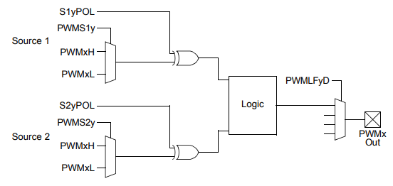
Using this feature ensures that only the corresponding secondary switch is activated when just the primary side is on, and it is truncated in sync with the associated primary switch. Additionally, it also suppresses any pulses generated by the two SOC triggers from the primary side.
    PG2CONbits.TRGMOD = 0b01; //re-trigable mode

    LOGCONAbits.PWMS1A = 0b0001; //PWM L 1
    LOGCONAbits.PWMS2A = 0b0011; //PWM L 2
    LOGCONAbits.PWMLFA = 0b01;  // AND
    LOGCONAbits.PWMLFAD = 0b001; // PWM2H

    LOGCONBbits.PWMS1B = 0b0000; //PWM H 1
    LOGCONBbits.PWMS2B = 0b0010; //PWM H 2
    LOGCONBbits.PWMLFB = 0b01;  // AND
    LOGCONBbits.PWMLFBD = 0b001; // PWM2L
A delay is introduced to ensure that the output current has increased sufficiently before the switch is turned on. During this delay period, the body diode conducts. Although the optimal delay value depends on the output load, a conservative fixed value is used to simplify the implementation.