
5.3 Targeting Higher Output Power
To reach a higher power level with the simple circuit we provide, we need complementary devices with a lower RON and/or a higher power dissipation capability, and fast transitions to cope with pulse widths in the 80 ns range. Furthermore, the input capacitance, gate charge and threshold voltage must be kept low enough to be driven with 3.3V CMOS ICs.
CSD16301Q2 and CSD25310Q2 were successfully tested, with the best results obtained by introducing LVCMOS buffers between the microprocessor I/Os and the power MOS gate serial resistors.
Schematics are provided for simulation in the Full_bridge_CSD16301-25310Q2_20ns_5%.wxsch and Full_bridge_CSD16301-25310Q2_20ns_95%.wxsch files, available in the MPLAB® Mindi™ Analog Simulator Software Library (see the Appendix).
The CSD16301Q2A and CSD25310Q2 SPICE models are available from the MPLAB® Mindi™ Analog Simulator Software Library. See the Appendix. Drag and drop the .lib files into the Mindi command shell as described in the Installation Guide referenced in the Appendix.
The ZHCS350 low-capacitance/low-loss Schottky diode limits the voltage drop in the PMOS gate drive compared to a regular Si diode. The ZHCS350 SPICE model is available in the MPLAB® Mindi™ Analog Simulator Software Library. See the Appendix.
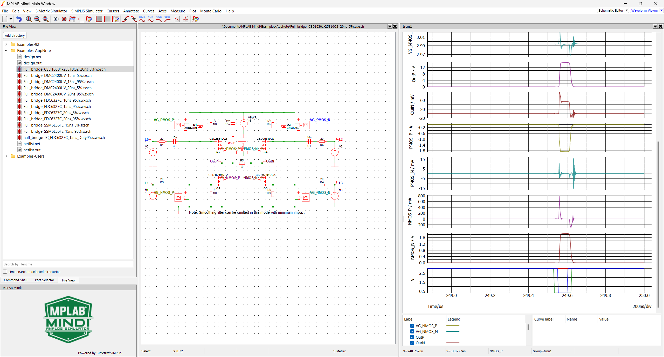
The waveforms show valid circuit behavior. The sharp positive output pulse is well rendered, and there is no violation of the device’s rated current. Losses align with the device data sheet values. Simulation shows an ON resistance of 30 mΩ in the PMOS (55 mV drop for 1.86A) and 30 mΩ in the NMOS (54 mV drop for 1.86A), which aligns with the typical values specified in the data sheet. Compared to an ideal 15V source, this generates a ~1.4% loss in the maximum power delivered to the 8Ω load. The dissipated power is ~100 mW per transistor, at most half of the time for AC operation, not taking into account any existing switching and inductor losses. With the 50°C/W Rth, the devices show a negligible 2.5°C heating when run at maximum power. Considering the maximum current capability in the 8~10A range and the 20V maximum voltage, the amplifier may be pushed to 18V with both 8Ω and 4Ω loads. It is also suitable to drive specialty 1Ω drivers such as Glass Acoustic Innovations BFC-D40-22-1-002, suitable for portable Bluetooth speakers directly powered from single Li-ion cells (3.6-4.2V).
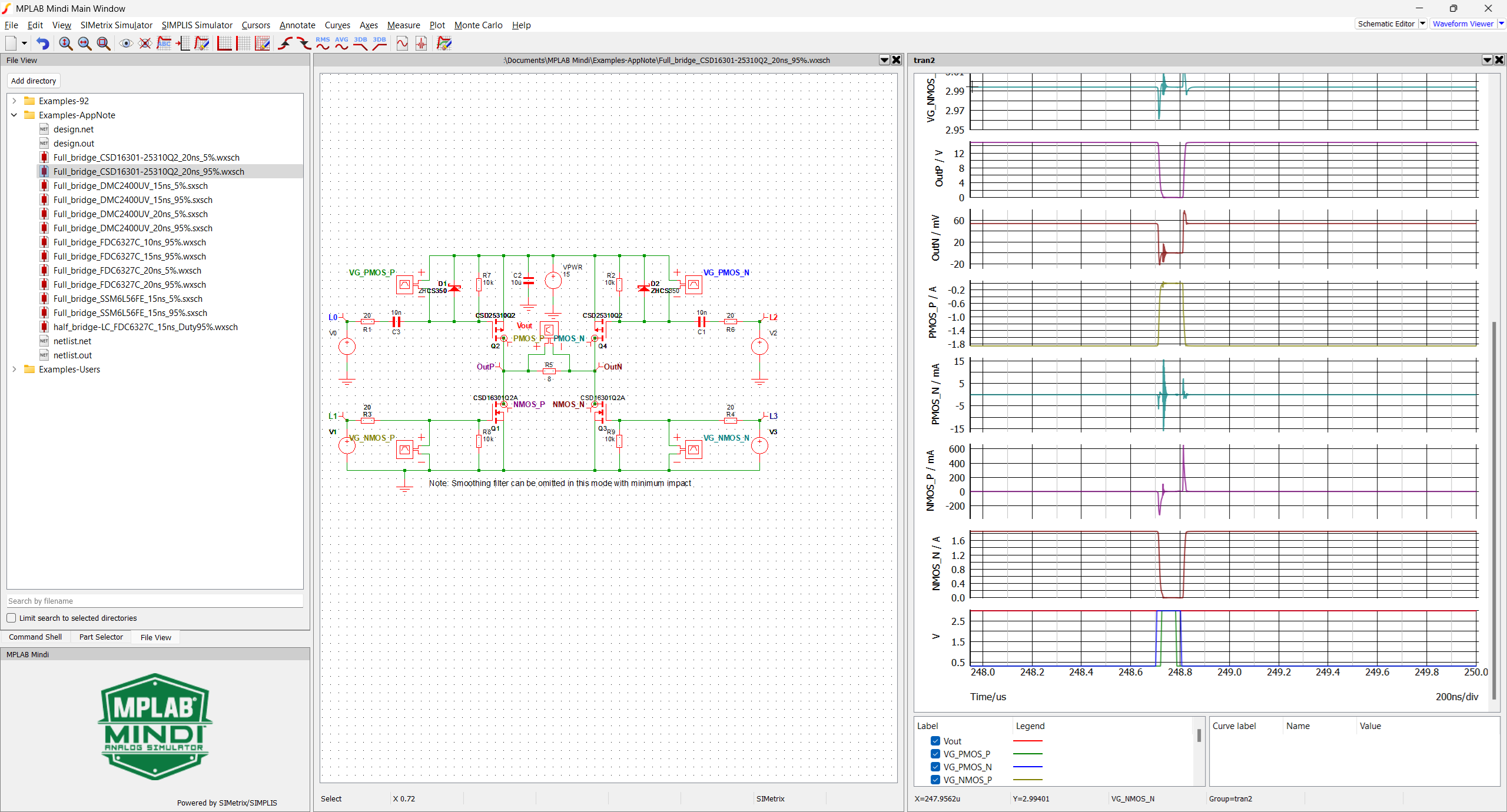
The results are valid, as in the 5% duty cycle case.