
5.2 Using Larger Dual Complementary Power Devices (SOT457, SC74, TSOP6)
The FDC6327C MOSFET, with a typical Ron of 100 mΩ for the NMOS, 200 mΩ for the PMOS and a total power dissipation of 700 mW, widens the operation range of the CLASS D in terms of supply voltage, output drive current and ambient temperature, at the cost of a slight area penalty.
To simulate a corresponding circuit with Mindi™, use the Full_bridge_FDC6327C_20ns_5%.sxsch and Full_bridge_FDC6327C_20ns_95%.sxsch files, available in the MPLAB® Mindi™ Analog Simulator Software Library. See the Appendix.
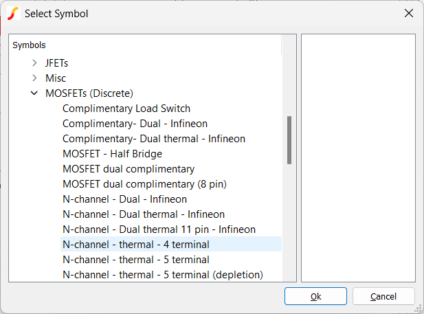
The SPICE model for the FDC6327C power device is also available (see the Appendix). Drag and drop the model into the Mindi command shell, as described in the Installation Guide referenced in the Appendix. This model senses the junction temperature through a fourth terminal and must be associated with the appropriate thermal, “4 terminal” MOS symbol in Mindi.
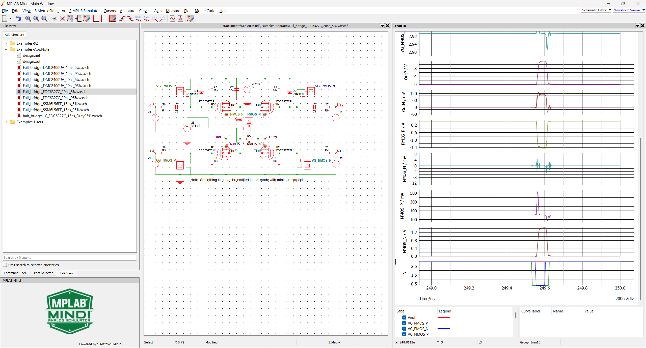
The waveforms show valid circuit behavior. The sharp positive output pulse is well rendered, and there is no violation of the device’s rated current. Losses are aligned with the device data sheet values. Simulation shows an ON resistance of 257 mΩ in the PMOS (0.37V drop for 1.44A) and 76 mΩ in the NMOS (109 mV drop for 1.44A), which is aligned with the device data sheet typical values. Compared to an ideal 12V source, this generates an ~8% loss in the maximum power delivered to the 8Ω load. The dissipated power is ~1W (shared between the two transistor pairs), not taking into account switching and inductor losses (if any). With a 65°C/W Rth for two transistor pairs, the device reaches a temperature of ≥135°C at 70°C ambient when run at maximum power.
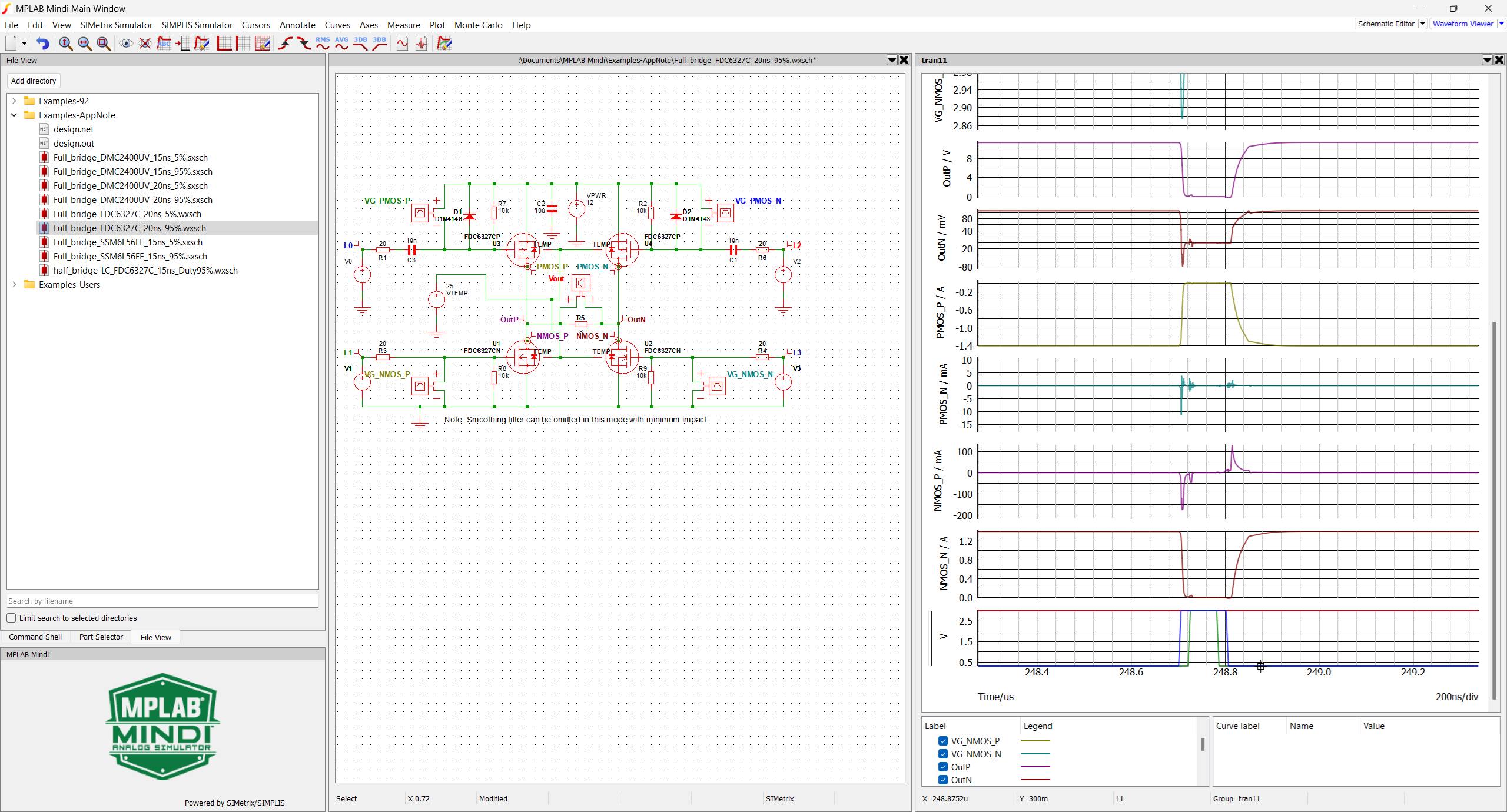
The waveforms show acceptable circuit behavior. The sharp negative output pulse is well rendered, though the rising edge is slightly slower than the falling edge. There is no violation of the device’s rated current. No improvement was achieved using 15 and 10 ns gaps, but as shoot-through current starts to grow, it is advised to keep the 20 ns setting. Raising the junction temperature to 130°C in simulation does not radically change behavior, but tends to lower the RON. This minimizes loss and avoids thermal breakdown, but increases the shoot-through current, though keeping it far from the maximum rating.
These power devices are not suitable for a supply greater than 12V with an 8Ω load, or greater than 7V with a 4Ω load, and these conditions cause a high temperature elevation if the maximum power is sustained.
Reliable operating conditions, including ambient temperatures up to 70°C, are up to 10V with an 8Ω load and up to 5V with a 4Ω load.