
5.1 Using Alternative Footprint-Compatible Power Devices (SOT563, SC89, SOT666)
The SSM6L56FE MOSFET was used in some Microchip microprocessor reference designs. To simulate a corresponding circuit with Mindi™, use the Full_bridge_SSM6L56FE_15ns_5%.sxsch and Full_bridge_SSM6L56FE_15ns_95%.sxsch files, available in the MPLAB® Mindi™ Analog Simulator Software Library. See the Appendix.
The SSM6L56FE power device SPICE model is available (see the Appendix). Drag and drop the .lib files into the Mindi command shell as described in the Installation Guide referenced in the Appendix.
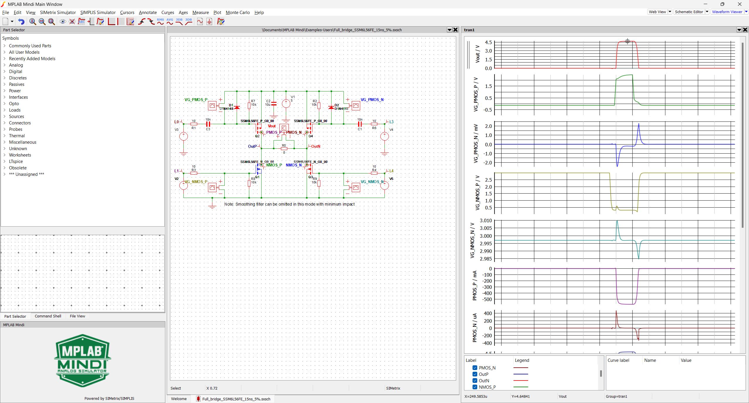
The waveforms show a sharp output pulse similar to the circuit in the original device data sheet. There is no violation of the device's rated current.
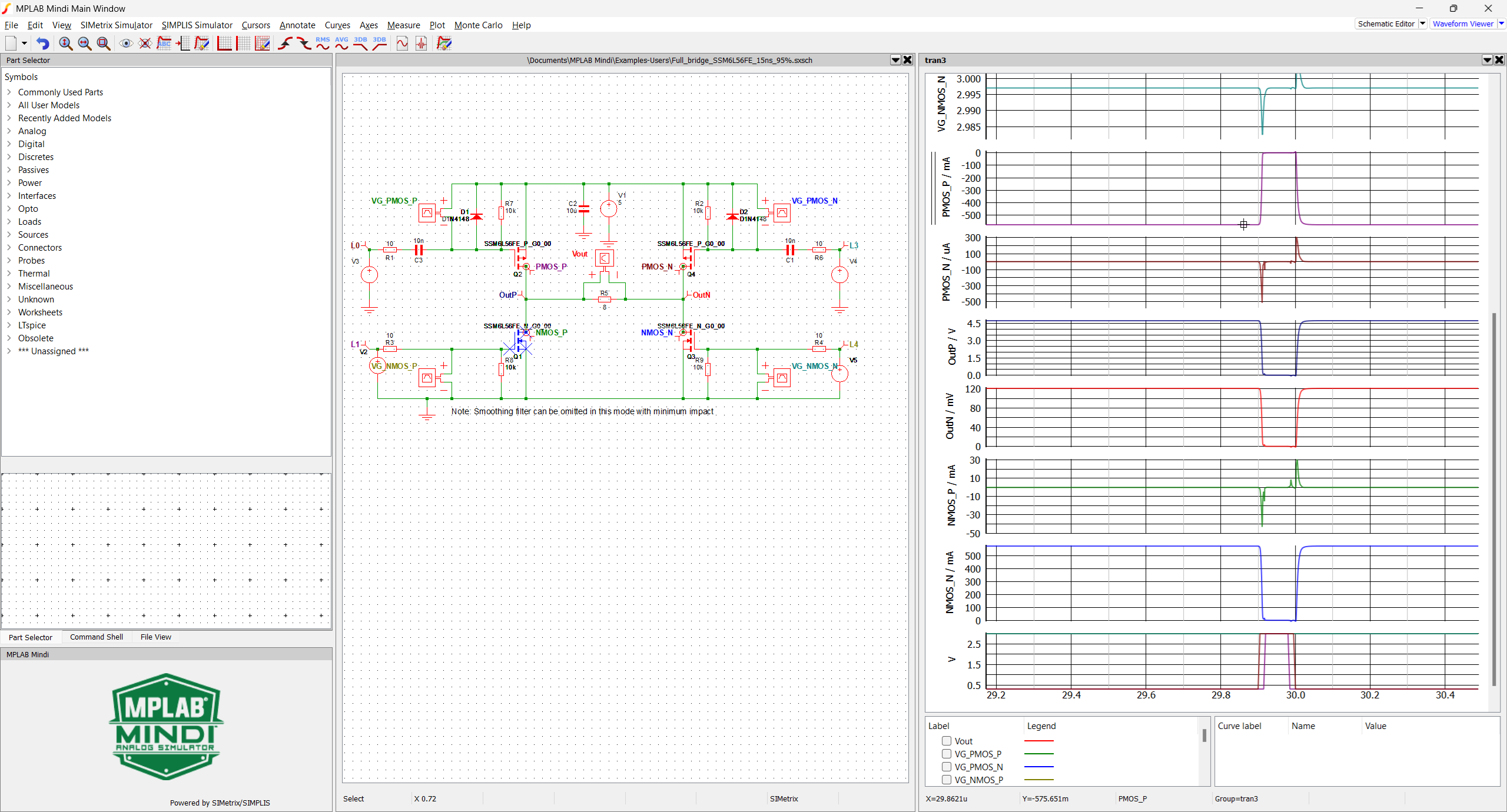
The 95% PWM duty cycle case shows no current surge. The 15 ns setting can be retained.
With an ON resistance of 0.4Ω in the PMOS (230 mV drop for 581 mA) and 0.2Ω in the NMOS (122 mV drop for 581 mA), the result is aligned with the typical values specified in the data sheet. Compared to an ideal 5V source, this generates a 14% loss in the maximum power delivered to the 8Ω load. The dissipated power is ~200 mW (shared between the two transistor pairs).
Losses are approximately halved compared to the original power device choice. The amplifier will play slightly louder. However, the increased Rth compared to the DMC2400UV dual transistor cancels out the benefit in terms of self-heating.