
5.5 DC-Coupled Audio DAC
For Use Case 3: Stereo Audio DAC with Active Differential to Single-Ended Low-Pass Filter, to utilize the differential input signal in order to suppress parasitic transient noise (“plops”), a novel approach is chosen. The suggested circuit is DC-coupled from input to output. A serial capacitor is used at the output to eliminate offset and other imperfections. This setup requires powering the operational amplifier with symmetrical supplies of ±2.5V. These supplies are derived from the 3.3V source, with the negative supply generated by a TC7660S charge pump.
As no SPICE model was available for this device, it was replaced by a behavioral circuit for the transient simulation, and an ideal 2.5V source was used for DC and AC simulation. The same behavioral model was applied to feed the input signal as used in the data sheet’s suggested circuit in Use Case 3: Stereo Audio DAC with Active Differential to Single-Ended Low-Pass Filter.
This can be simulated with Mindi using the 4th_order_differential_to_SE_active_filter_AC&DCwxsch and 4th_order_differential_to_SE_active_filter_TRAN.wxsch files, available from the MPLAB® Mindi™ Analog Simulator Software Library. See the Appendix.
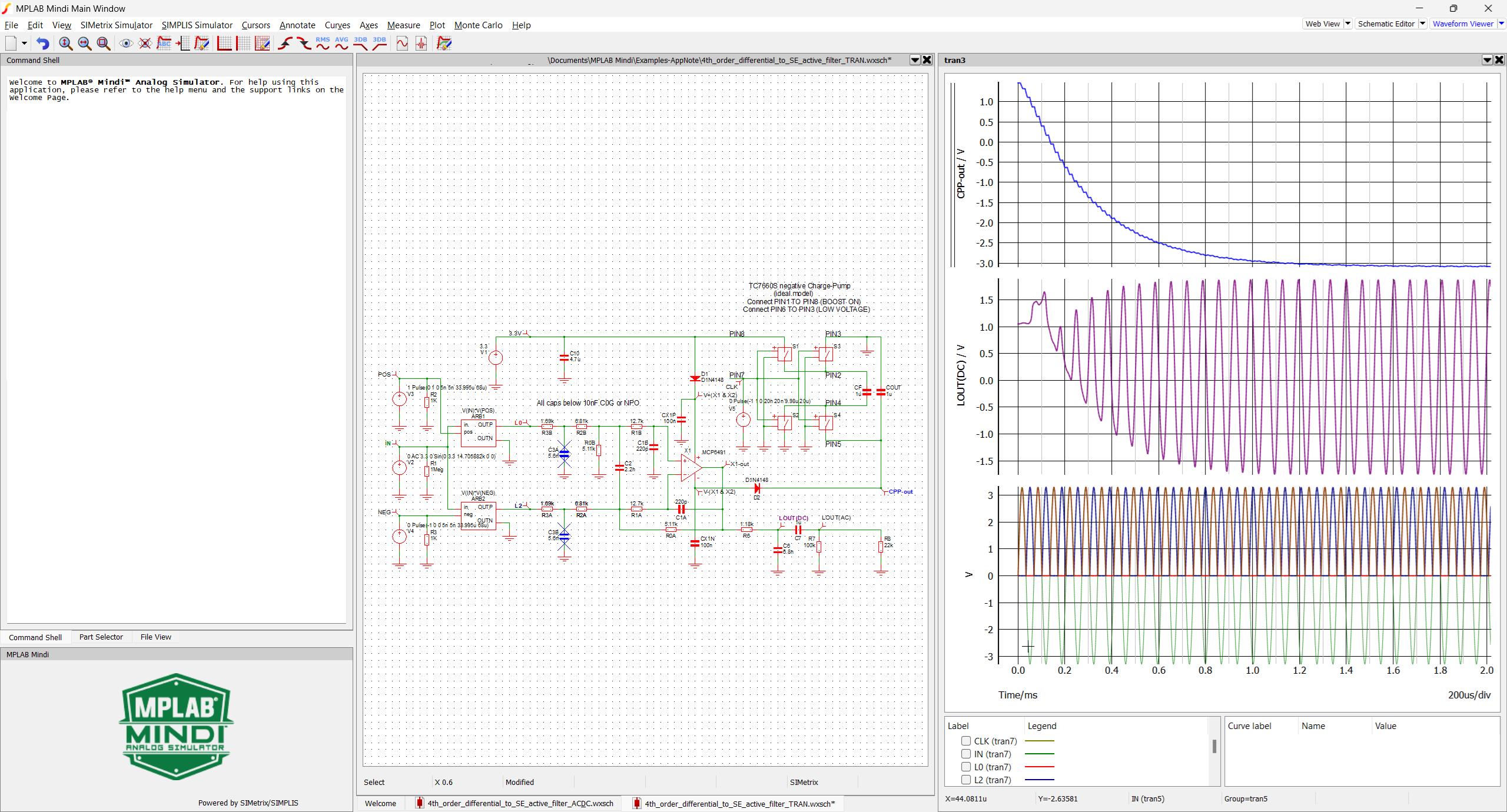
The L0 and L2 signals are not modeled as PWM but as the resulting average. The main characteristic is that L0 generates the positive half of the signal and L2 generates the negative half. This is achieved by synchronously slicing the IN sine wave. The amplifier must recombine both and suppress the high-frequency components from the PWM/ΔΣ.
The charge pump quickly powers the operational amplifier, and the output transient is moderate. The operational amplifier output swing is centered within the ±2.5V range, with some guard bands.
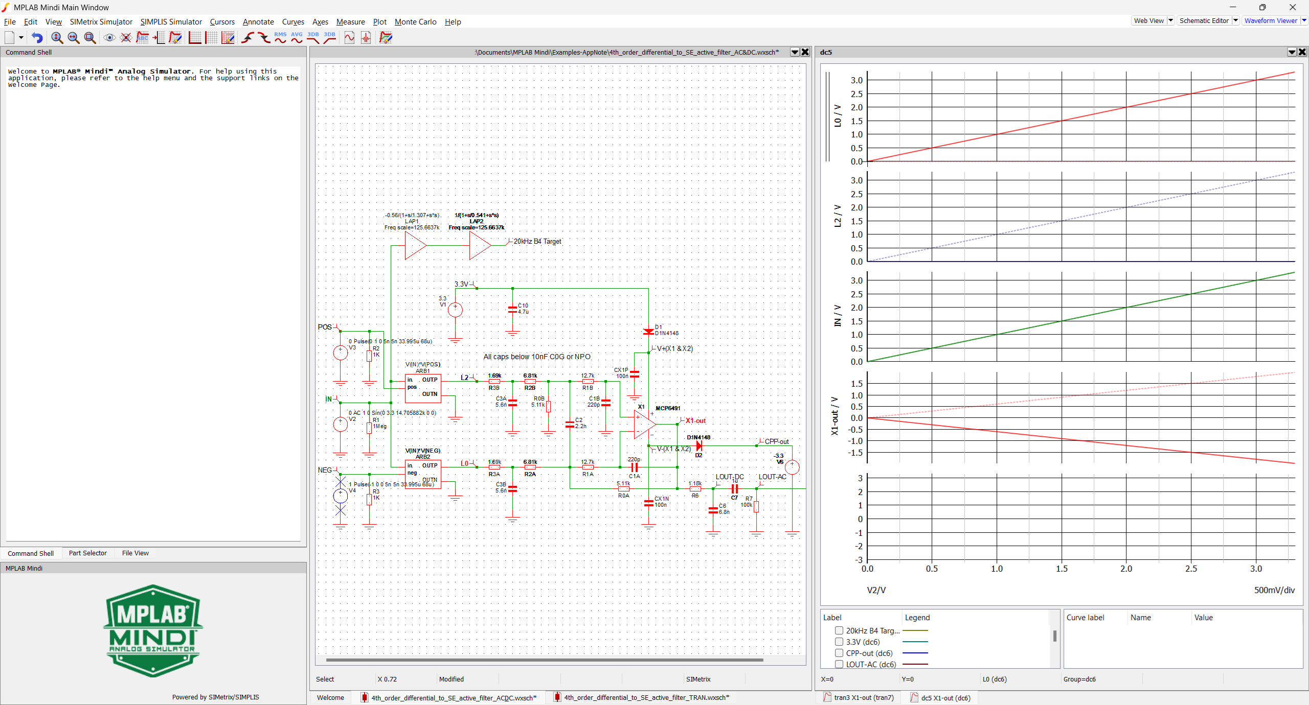
Two runs are required to explore the whole system range: one with the V3 DC value set to 0 and one with V4 set to 1, as represented in Figure 5-9, where the results are shown with solid line traces. One run with inverted settings was executed just before and is represented by the dotted line traces. The output ranges from -2.2 to 2.2 V.
The AC transfer function matches a 20 kHz fourth-order Butterworth low-pass filter with a -0.56 gain, chosen to avoid amplifier saturation, even during transients. The cut-off frequency, as well as the gain, can be tailored to the application using the filter calculator provided together with a schematic and a simulation bench for Mindi. See the Appendix.
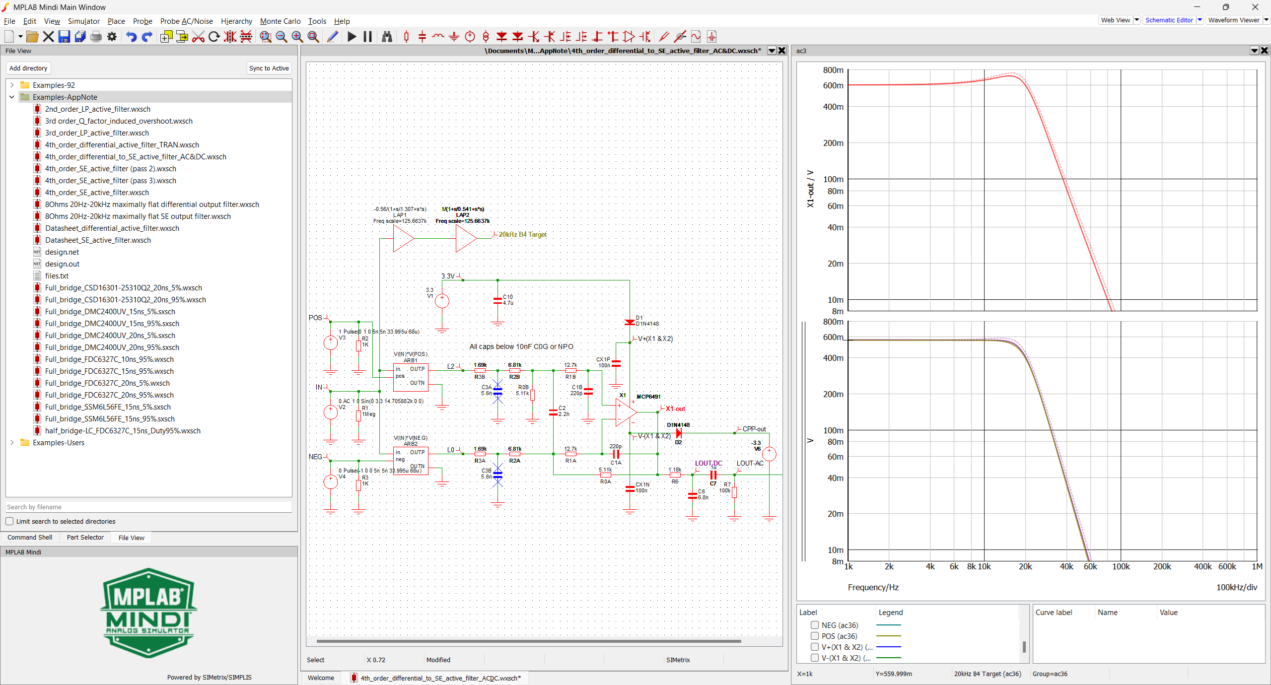
For the AC response, the transfer function can be measured from the L0 or L2 input by varying the V3 and V4 settings. The results are the same for both inputs (except for the sign). As mentioned in the filter calculator, the passive R3x-C3x input cells interact with the second-order active low-pass filter, which is not fully taken into account in the passive components’ computation. Thus, the effective transfer function differs slightly from the target. Tuning C3x in the simulation is generally the best way to match the prototype filter. Here, the 4.7 nF-computed value results in the dotted line trace. Changing C3A and C3B from 4.7 to 5.6 nF matches the theoretical fourth-order Butterworth (B4) filter. Refer to the Flexible Third-Order Component Computation section for further details.
The table below provides an overview of the filter calculator. Step 1 describes the requested second-order filter (see Alternative Third-Order Component Computation for further details) and the circuit constraints. It results in a set of outputs to guide final choices, including some warnings related to overshoots that help avoid saturation during transients and/or at resonance frequency (if any). Step 2 allows the user to set the primary component values and computes the remaining values.
| Parameters | Value | Unit | Warnings/Suggested Normalized Values | ||||
|---|---|---|---|---|---|---|---|
| Step 1 | Inputs | Fc = | 20000 | Hz |
WARNING: Q>0.5 generates a peak in the step response that must be taken into account in the maximum gain computation to avoid saturating the amplifier output. Reduce the global gain according to the step overshoot and check the transient simulation results. WARNING: Q>1 generates a gain peak at resonance that must be taken into account to avoid saturating the amplifier output. Reduce global gain according to the gain at resonance frequency and check AC simulation results. Do not cumulate step overshoot and extra gain at resonance frequency correction: apply the highest values from both. | ||
| Q = | 1.41 | – | |||||
| INmin = | -3.3 | V | |||||
| INmax = | 3.3 | V | |||||
| OUTmin = | -2.45 | V | |||||
| OUTmax = | 2.45 | V | |||||
| Capacitor series = | 12 | – | |||||
| Resistor series = | 96 | – | |||||
| Outputs | No sat. |G|max = | 0.74 | – | ||||
| Resonance freq = | 15824 | Hz | |||||
| Extra gain @Fr = | 1.17 | – | |||||
| Step overshoot = | 1.18 | – | |||||
| Min(C2/C1) = | 6.97 | – | |||||
| Suggested C1 = | 1.20E-10 | F | |||||
| Suggested C2 = | 1.00E-09 | F | |||||
| Step 2 | Inputs | Select |G| = | 0.6 | – | |||
| Select R7 = | 1.00E+05 | Ω | |||||
| Select R8 = | 2.20E+04 | Ω | |||||
| Select C1 = | 2.20E-10 | F | |||||
| Select C2 = | 2.20E-09 | F | |||||
| Select C6 = | 6.80E-09 | F | |||||
| Outputs | Min(C2/C1) = | 6.40 | – | ||||
| Computed R0 = | 5.12E+03 | Ω | Nearest value from R0 in E96 series = | 5110 | Ω | ||
| Computed R1 = | 1.28E+04 | Ω | Nearest value from R1 in E96 series = | 12700 | Ω | ||
| Computed R2 = | 6.82E+03 | Ω | Nearest value from R2 in E96 series = | 6810 | Ω | ||
| Computed R3 = | 1.71E+03 | Ω | Nearest value from R3 in E96 series = | 1690 | Ω | ||
| Computed R6 = | 1.17E+03 | Ω | Nearest value from R6 in E96 series = | 1180 | Ω | ||
| Computed C3 = | 4.67E-09 | F | Nearest value from C3 in E12 series = | 4.6 | nF | ||
| Computed C7 = | 8.83E-07 | F | Nearest value from C7 in E12 series = | 830 | nF | ||
| R6 induced loss = | 0.94 | – | Effective overall gain = | -0.56 | – | ||