1.2 Electrical Characteristics
The following table lists the electrical characteristics of the gate driver.
| Parameter | Description | Min. | Typ. | Max. | Unit |
|---|---|---|---|---|---|
| Power Supply | |||||
|
Supply voltage |
VCC to GND |
14 |
15 |
16 |
V |
|
Supply current |
Without load | — |
110 | — |
mA |
|
Supply current |
With load3 | — | — |
1250 |
mA |
|
UVLO level—HI and LO5 |
Primary side low voltage detect fault level |
13.5 |
14 | — |
V |
|
UVLO level—HI and LO5 |
Secondary side low voltage detect fault level3 |
20 | — | — |
V |
|
OVLO level—HI and LO5 |
Primary side high voltage detect fault level | — |
16 |
16.5 |
V |
|
VSOFT5 |
Two-level turn-off3 | — |
1.5 | — |
V |
|
VSOFTD15 |
DSAT first level turn-off voltage3 | — |
9 | — |
V |
|
VSOFTD25 |
DSAT second level turn-off voltage3 | — |
5 | — |
V |
| Signal I/O | |||||
|
Input impedance |
5V—HI and LO side input | — |
500 | — |
Ω |
|
15V—HI and LO side input | — |
3000 | — | ||
|
5V differential—HI and LO side input | — |
1000 | — | ||
|
VIN low |
5V—turn-off threshold | — | — |
1.25 |
V |
|
15V—turn-off threshold | — | — |
4 | ||
|
VIN high |
5V—turn-on threshold |
3.5 | — | — |
V |
|
15V—turn-on threshold |
10 | — | — | ||
|
VIN (differential option) |
Difference between VIN+ to VIN- |
2 | — | — |
V |
|
Gate output voltage low3 | — |
-6 | — |
-4 |
V |
|
Gate output voltage high3 | — |
17 | — |
21 |
V |
|
Fault output voltage |
Fault lines are open collect with 5 mA load |
0.3 | — | — |
V |
|
Fault output current4 | — | — | — |
10 |
mA |
|
Switching frequency2 | — | — | — |
200 |
kHz |
|
DC link and temperature monitoring |
High Voltage (HV) and temp monitoring output |
0 | — |
5 |
V |
|
DC link and temperature monitoring |
PWM frequency | — |
31.5 | — |
kHz |
|
DC link and temperature monitoring |
Output impedance | — |
510 1% | — |
Ω |
|
DC link voltage | — |
880 | — |
920 |
V |
|
Temperature trip | — | — |
125 | — |
°C |
| MOSFET Short Protection | |||||
|
Desat monitor voltage5 |
Between drain and sink of MOSFET3 | — |
8.25 | — |
V |
|
TDSAT5 |
Activation after MOSFET turn-on | — |
1.5 | — |
μs |
|
Response time after fault | — | — | — |
200 |
ns |
- The input signal must not be activated until 20 ms after power is applied to allow the on-board DC-DC converter to stabilize.
- The actual maximum switching frequency is a function of gate capacitance.
- Dependent on SiC MOSFET with Qg = 1025 nC, Vth = 2.9V, and Ciss = 19.5 nF.
- Fault lines are open collector and require a pull-up resistor, 2 kΩ recommended.
- Software configurable parameter.
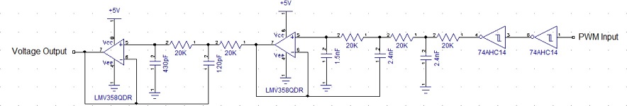
Temperature and High Voltage PWM Monitoring: The gate driver provides two 31.5 kHz, 5V PWM output signals that monitor the thermistor temperature (non-isolated) and the DC link voltage (isolated) (high-side drain to low-side source) of the SiC MOSFET power module. The PWM signals have an output impedance of 510Ω. When combined with an external low-pass filter, these signals represent a real-time, isolated voltage for both high voltage and thermistor temperature. A sallen-key active low-pass filter can be used with these outputs, as shown in the following figure with a 2 kHz cut-off frequency. The cut-off frequency is optimized for your application. For simplicity, a simple RC low-pass filter with a 100 Hz cut-off frequency is also used.
The following figure shows an example of external 2 kHz low-pass filter.