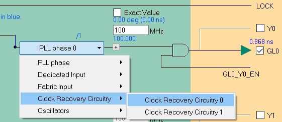
2.4.1 Output Clocks Selection
You must select at least one of the four output clocks. The GL0, GL1, GL2, and GL3 clocks drive a global network in the FPGA fabric; Y0, Y1, Y2, and Y3 drive local routing resources in the FPGA fabric.

The source of the GL[x]/Y[x] clocks can be:
- PLL —The PLL block offers eight
phases (0° to 315° in 45° steps). The actual phases
are highlighted in blue on the configurator dialog.
The actual phase is not the same as the selected
phase if the output divider is not 1
(
actual_phase = selected_phase /
                                                  output_divider
). - Dedicated Input Pad —The clock source is one of the four regular FPGA I/Os that have a dedicated path to the CCC. The Configure as differential option allows you to configure any dedicated Input Pad as differential I/O. The package pin names for the selected location are displayed next to the dedicated pads.
- FPGA Fabric Input —The clock source is one of the four fabric input signals coming from the FPGA Fabric.
- Clock Recovery Circuitry —Two RX Clock Recovery Circuitry blocks are available—Block 0 and Block 1—for each CCC. If the CCC needs to connect to Spacewire or Glitch Filter, configure the source of your GL[x] to use the Clock Recovery Circuitry. The GL[x] output can then be used.
- Oscillators —The source is from the on-chip 50 MHz oscillator. The RCOSC_50MHZ macro must be manually instantiated and connected to the CCC input pin if selected as the reference clock source.
