Signal integrity issues on CA or DQ lines. When the Write Leveling training fails, a dialog box
appears as shown in the following figure.Figure 3-8. Write Leveling
Training Fail
Workaround
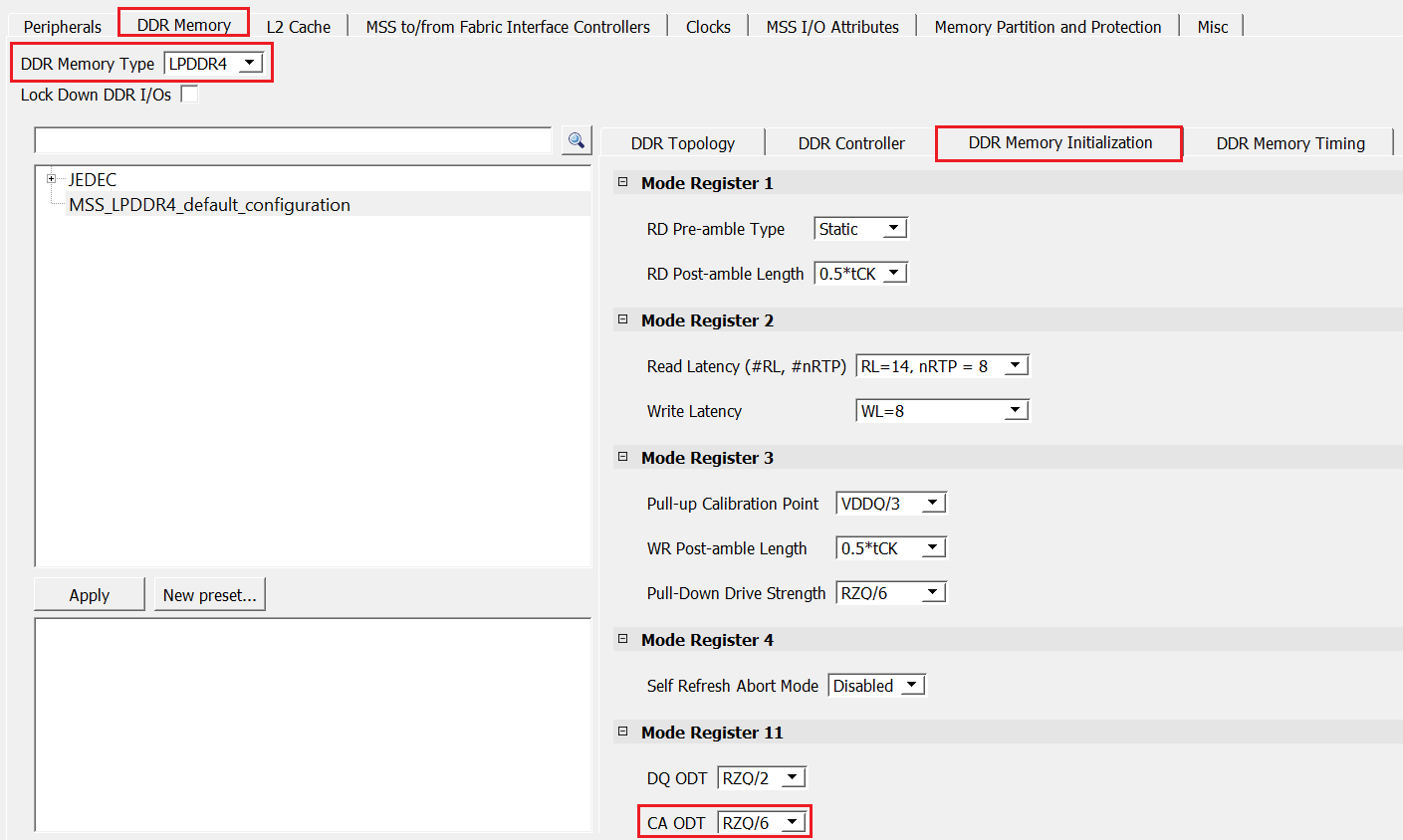
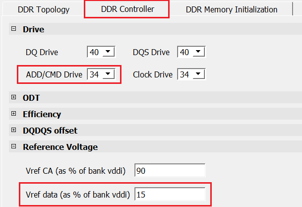
Configure any one of the following parameters to a different value using the MSS Configurator when the Write Leveling training fails:
Memory CA ODT
FPGA ADD/CMD Drive
FPGA Vref data (as % of bank vddi)
The following figure shows the configuration of CA ODT in the DDR Memory Initialization tab.Figure 3-9. Configuring CA ODT—DDR Memory Initialization TabThe following figure shows the configuration of ADD/CMD drive or Vref data in the DDR Controller tab.Figure 3-10. Configuring ADD/CMD Drive or Vref Data—DDR Controller Tab