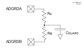
32.4.4 Guard Ring Outputs
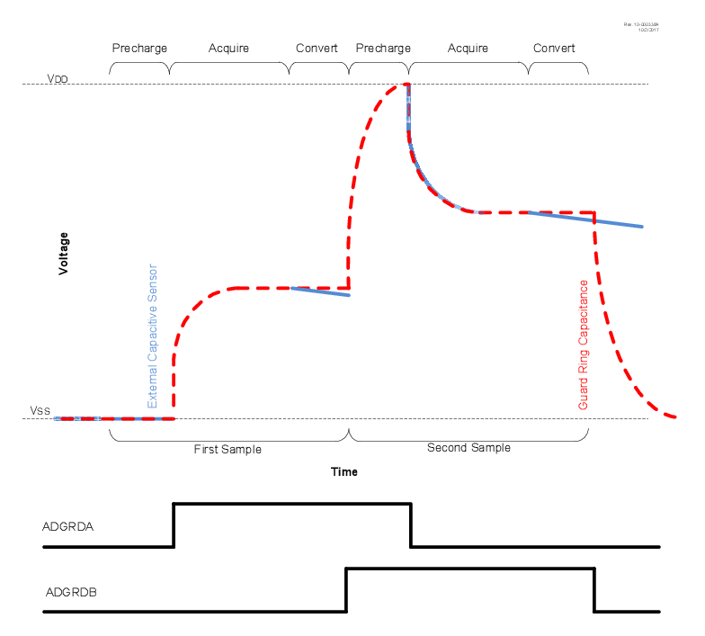
Figure 32-8 shows a typical guard ring circuit. CGUARD represents the capacitance of the guard ring trace placed on the PCB board. The user selects values for RA and RB that will create a voltage profile on CGUARD, which will match the selected acquisition channel.
The purpose of the guard ring is to generate a signal in phase with the CVD sensing signal to minimize the effects of the parasitic capacitance on sensing electrodes. It also can be used as a mutual drive for mutual capacitive sensing. For more information about active guard and mutual drive, see AN1478, “mTouchTMSensingSolution Acquisition Methods Capacitive Voltage Divider”.
The ADC has two guard ring drive outputs, ADGRDA and ADGRDB. These outputs can be routed through PPS controls to I/O pins (see “Peripheral Pin Select (PPS) Module” for details). The polarity of these outputs are controlled by the ADGPOL and ADIPEN bits.
At the start of the first precharge stage, both outputs are set to match the ADGPOL bit. Once the acquisition stage begins, ADGRDA changes polarity, while ADGRDB remains unchanged. When performing a double sample conversion, setting the ADIPEN bit causes both guard ring outputs to transition to the opposite polarity of ADGPOL at the start of the second precharge stage, and ADGRDA toggles again for the second acquisition. For more information on the timing of the guard ring output, refer to Figure 32-8 and Figure 32-9.