
18.6.5 Phase Locked Loop (PLL) Operation
Important: Before attempting to
initialize and enable either of the two PLL's, the user must first enable the internal
PLL regulator, SUPC.VREGCTRL.AVREGEN, and then wait a minimum of 55µs for internal power
to stabilize before reading or writing any of the PLL registers. The internal BOOT ROM
code may already have enabled the PLL so user should first check if PLL regulator has
already been enabled.
Important:
To achieve stable operation of the PLL as a primary clock source across temperature,
the following procedure should be followed.
- PLL0 must be dedicated to the CPU.
- PLL0 must be stepped up to the operating frequency in <= 75 MHz increments.
- The step delay needs to be >= 1 us.
The PLL provides a wide range of outputs from 12.7 MHz to 1600 MHz with, (i.e. FCLK_PLL max = 300Mhz), support for input reference clock ranges from 4 MHz to 48 MHz. The PLL maintains a locked phase between the VCO input (reference) signal FPDF and the respective VCO output frequency FVCO via phase comparison and frequency multiplication.
The clock(s) from the PLL output(s), (CLK_PLLx_300n) is a source for the Generic Clock module (GCLK).
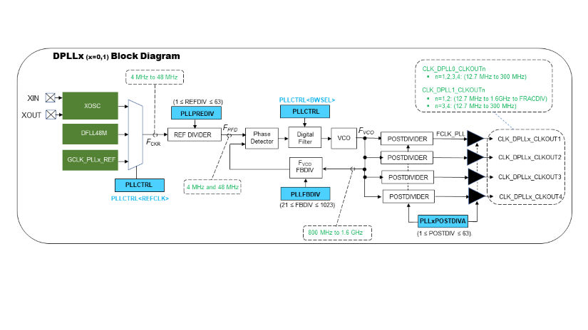
Important: The frequency
generated by the PLL oscillator can be up to 1600 MHz but is limited to 300 MHz (max)
for everything except inputs to FRACTIONAL DIVIDER. Depending on the operating
conditions of the product using the PLL, the maximum allowed frequency can be as low as
12.7 MHz. Refer to the electrical characteristics of the product for a safe
configuration of the PLL controller.