5.2.1 Power-up
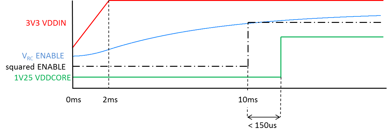
VDDIO, VDDIN and VDDAMP must rise simultaneously, prior to VDDCORE and VDDPLL rising. This is respected if VDDCORE and VDDPLL are supplied by the embedded voltage regulator and the voltage regulator is turned on after VDDIN reaches 3.3V.
The figure below shows system response when an RC delay line (R = 6K8Ω, C = 1 µF) is used to derive ENABLE control from VDDIN.

Although no special power-up sequence is required between high-voltage PVDDAMP power domain and low-voltage domain (VDDIO, VDDIN and VDDAMP), it is recommended to satisfy the ramp-up slopes defined in Table 5-2. The PL460 is designed to operate properly either with PVDDAMP pins powered-up while the low-voltage domain is not available as well as the other way around.
| Parameter | Min | Typ | Max | Unit |
|---|---|---|---|---|
| 3.3V power supply ramp-up slope (1), (2) | 0.6 | — | 24 | V/ms |
| PVDDAMP power supply ramp-up slope (1), (3) | 1.5 | — | 16 | V/ms |
- Power supply ramp-up slope recommended values take into account the recommended decoupling networks to be used on each supply rail, as well as output current capability of power supplies typically used in smart metering applications.
- VDDAMP pins connected at the PCB level.
- PVDDAMP pins connected at the PCB level.
