
4.4.2 Flexible Third-Order Component Computation
Using the filter design tool (Excel spreadsheet) available in the MPLAB® Mindi™ Analog Simulator Software Library (see the Appendix), we calculated a 20 kHz low-pass Butterworth filter. The filter has a Q factor of 1 for the second-order cell and is set for maximum gain. The supply voltages and operational amplifier limitations regarding rail-to-rail operation are taken into account. The simulation bench is available as the file 3rd_order_LP_active_filter.wxsch in the Library.
Compared to the static maximum gain computed using the Excel spreadsheet, the gain was slightly reduced to take into account the small overshoot in the step response. This is done through Step 2 inputs, as well as by choosing capacitor values that are easier to find (while complying with the constraint on C2/C1 and with the penalty of lower resistor values).
| Parameters | Value | Unit | Warnings/Suggested Normalized Values | ||||
|---|---|---|---|---|---|---|---|
| Step 1 | Inputs | Fc (Hz) = | 20000 | Hz | WARNING: Q>0.5 generates a peak in the step response that must be taken into account in the max gain computation to avoid saturating the amplifier output. Reduce global gain according to the step overshoot and check transient simulation results. | ||
| Q = | 1.00 | – | |||||
| INmin = | 0 | V | |||||
| INmax = | 3.3 | V | |||||
| OUTmin = | 0.05 | V | |||||
| OUTmax = | 4.95 | V | |||||
| V1 = | 5 | – | |||||
| Channels count = | 1 | – | |||||
| Capacitors series = | 12 | – | |||||
| Resistors series = | 96 | – | |||||
| Outputs | No sat. |G| max = | 1.48 | – | ||||
| Resonance freq = | NONE | Hz | |||||
| Extra gain @Fr = | 1.00 | – | |||||
| Step overshoot = | 1.08 | – | |||||
| Min(C2/C1) = | 9.94 | – | |||||
| Suggested C1 = | 1.50E-10 | F | |||||
| Suggested C2 = | 2.60E-09 | F | |||||
| Step 2 | Inputs | Select |G| = | 1.3 | – | |||
| Select C1 = | 2.20E-10 | F | |||||
| Select C2 = | 2.20E-09 | F | |||||
| Outputs | Min(C2/C1) = | 9.20 | – | ||||
| Computed R0 = | 1.30E+04 | Ω | Nearest value from R0 in E96 series = | 13000 | Ω | ||
| Computed R1 = | 1.01E+04 | Ω | Nearest value from R1 in E96 series = | 10000 | Ω | ||
| Computed R2 = | 7.98E+03 | Ω | Nearest value from R2 in E96 series = | 8060 | Ω | ||
| Computed R3 = | 2.00E+03 | Ω | Nearest value from R3 in E96 series = | 2000 | Ω | ||
| Computed R4 = | 2.64E+04 | Ω | Nearest value from R4 in E96 series = | 26100 | Ω | ||
| Computed R5 = | 3.89E+04 | Ω | Nearest value from R5 in E96 series = | 39200 | Ω | ||
| Computed C3 = | 3.99E-09 | F | Nearest value from C3 in E12 series = | 3.8 | nF | ||
| Computed C4 = | 1.01E-06 | F | Nearest value from C4 in E12 series = | 1000 | nF | ||
The theoretical maximum gain obtained by mapping the input range onto the output range (1.48 in this case) is reduced to take into account the dynamic behavior during transients, as the expected overshoot is a factor of 1.08 for Q=1.
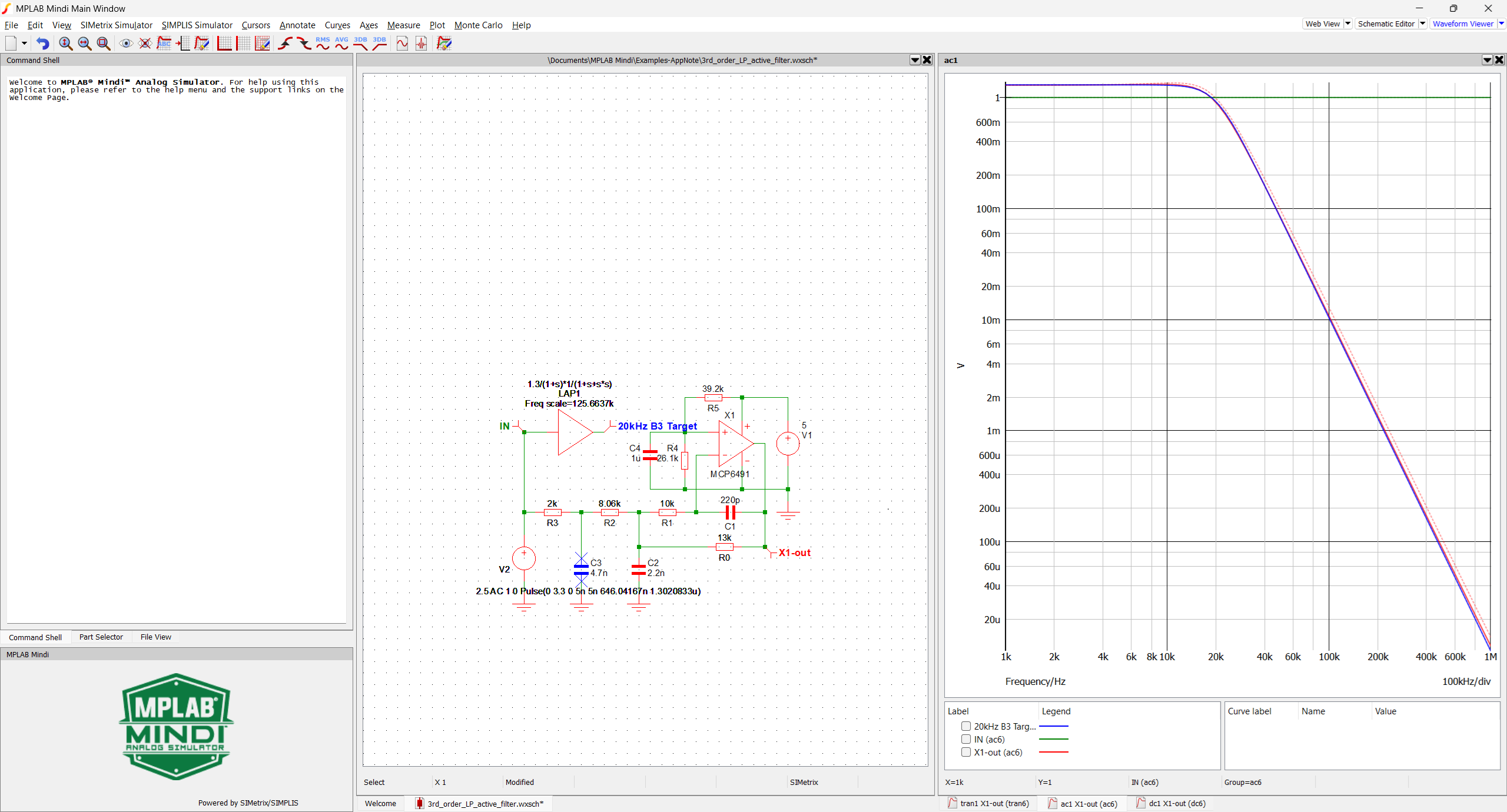
The values computed by the filter calculator generate the response shown as a dashed line, which is quite close to the target response in blue. Changing the C3 capacitor from 3.9 nF to 4.7 nF brings the response to the target.
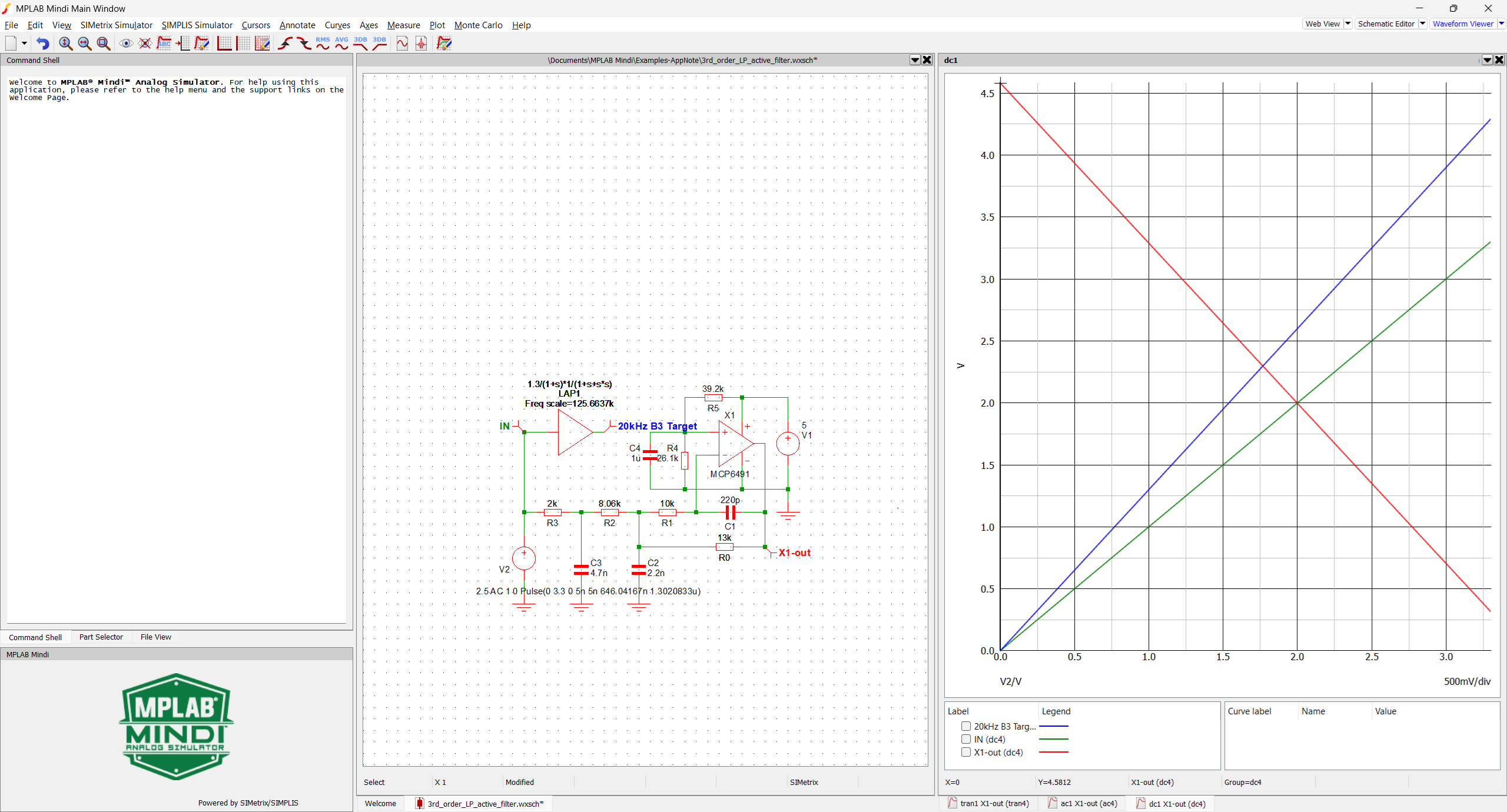
The DC simulation shows that applying the [0, 3.3V] input range (green curve) generates an output range close to [0, 5V] (red curve), with some rather symmetrical ~300 mV guard bands for supply voltage variation, overshoot and imperfect rail-to-rail operation. It also shows the negative gain compared to the ideal transfer function block (blue curve). As for the second order described in the previous chapter, the circuit must be AC-coupled to the receiver.
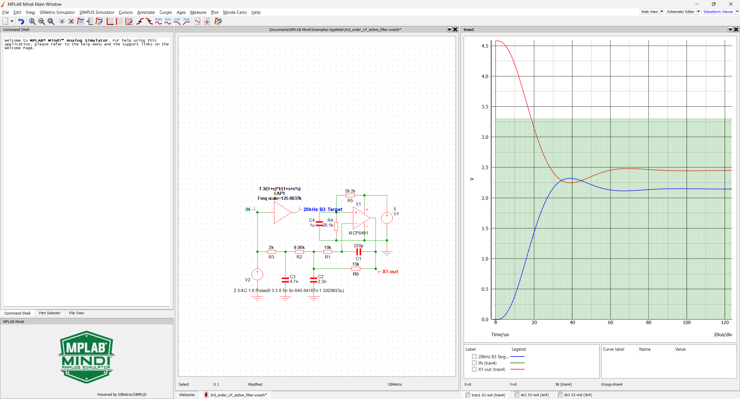
Dynamic behavior is as expected. For the ideal B3 filter, the peak value for the 1.65V input (3.3V*50%) is 1.65*1.3*1.08=2.32V. Starting from 4.58V, the simulated circuit decreases to 2.25V, which is a -2.33V step. The Steady state is 2.45V, which is a -2.13V variation, to be compared with the 1.65*1.3=2.145V target.