
4.4.4 Flexible Fourth-Order Component Computation
To enhance the device data sheet reference design, the Q factor is set to √2 to generate a quasi-B4 filter, as described in Use Case 3 Output Filter Computation.
Additionally, the gain can be adjusted to better suit the needs of the application:
- The full scale can be adjusted to target the standard line level, which is a maximum of 0.775 VRMS. With a 3.3V level at the PWM output, the gain should be set to 0.775/(3.3/2√2) = 0.66.
- Alternatively, the dynamic range can be maximized. To achieve this, match the gain and offset of the circuit for the Class D pulse magnitude (for its given supply voltage, generally 3.3V) to create a full swing at the operational amplifier output (for its given supply voltage). This feature is already built into the filter calculator, as described previously, and used as a first guess to estimate various key component values.
The simulation bench is available as the file 4th_order_SE_active_filter.wxsch, along with the filter calculator (Excel spreadsheet), in the MPLAB® Mindi™ Analog Simulator Software Library. See the Appendix.
| Parameters | Value | Unit | Warnings/Suggested Normalized Values | ||||
|---|---|---|---|---|---|---|---|
| Step 1 | Inputs | Fc (Hz) = | 20000 | Hz |
WARNING: Q>0.5 generates a peak in step response that must be taken into account in max gain computation not to saturate the amplifier output. Reduce global gain according to the step overshoot and check transient simulation results. WARNING: Q>1 generates a gain peak at resonance that must be taken into account to avoid saturating the amplifier output. Reduce global gain according to the gain at the resonance frequency and check AC simulation results. Do not cumulate step overshoot and extra gain at resonance frequency correction: apply the highest values from both. | ||
| Q = | 1.41 | – | |||||
| INmin = | 0 | V | |||||
| INmax = | 3.3 | V | |||||
| OUTmin = | 0.05 | V | |||||
| OUTmax = | 4.95 | V | |||||
| V1 = | 5 | – | |||||
| Channels count = | 1 | – | |||||
| Capacitors series = | 12 | – | |||||
| Resistors series = | 96 | – | |||||
| Outputs | No sat. |G| max = | 1.48 | – | ||||
| Resonance freq = | 15824 | Hz | |||||
| Extra gain @Fr = | 1.17 | – | |||||
| Step overshoot = | 1.18 | – | |||||
| Min(C2/C1) = | 19.88 | – | |||||
| Suggested C1 = | 1.00E-10 | F | |||||
| Suggested C2 = | 4.60E-09 | F | |||||
| Step 2 | Inputs | Select |G| = | 1.2 | – | |||
| Select R7 = | 1.00E+05 | Ω | |||||
| Select R8 = | 2.20E+04 | Ω | |||||
| Select C1 = | 2.20E-10 | F | |||||
| Select C2 = | 4.70E-09 | F | |||||
| Select C6 = | 6.80E-09 | F | |||||
| Outputs | Min(C2/C1) = | 17.60 | – | ||||
| Computed R0 = | 7.42E+03 | Ω | Nearest value from R0 in E96 series = | 7500 | Ω | ||
| Computed R1 = | 8.25E+03 | Ω | Nearest value from R1 in E96 series = | 8250 | Ω | ||
| Computed R2 = | 4.95E+03 | Ω | Nearest value from R2 in E96 series = | 4990 | Ω | ||
| Computed R3 = | 1.24E+03 | Ω | Nearest value from R3 in E96 series = | 1240 | Ω | ||
| Computed R4 = | 1.96E+04 | Ω | Nearest value from R4 in E96 series = | 19600 | Ω | ||
| Computed R5 = | 2.85E+04 | Ω | Nearest value from R5 in E96 series = | 28700 | Ω | ||
| Computed R6 = | 1.17E+03 | Ω | Nearest value from R6 in E96 series = | 1180 | Ω | ||
| Computed C3 = | 6.43E-09 | Ω | Nearest value from C3 in E12 series = | 6.8 | nF | ||
| Computed C4 = | 1.37E-06 | F | Nearest value from C4 in E12 series = | 1500 | nF | ||
| Computed C7 = | 8.83E-07 | F | Nearest value from C7 in E12 series = | 830 | nF | ||
| R6 induced loss = | 0.94 | – | Effective overall gain = | -1.13 | – | ||
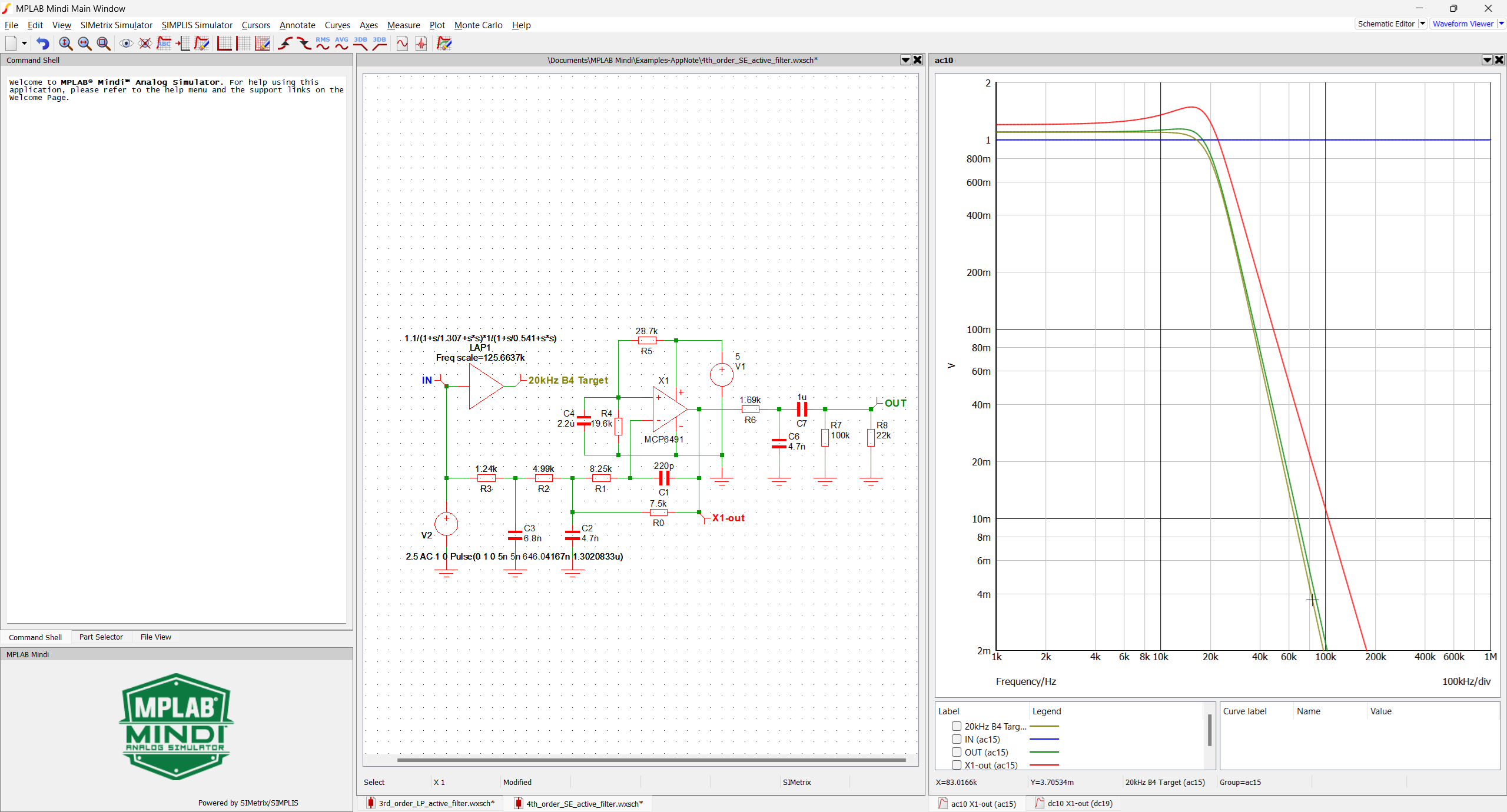
As shown, the response is quite close to the Butterworth target. Some extra damping will help. As mentioned in the filter calculator for the third and fourth orders, the upfront passive first-order cell interferes with the second-order cell. Experience shows that adjusting the C3 value is the best way to bring the behavior back to the target.
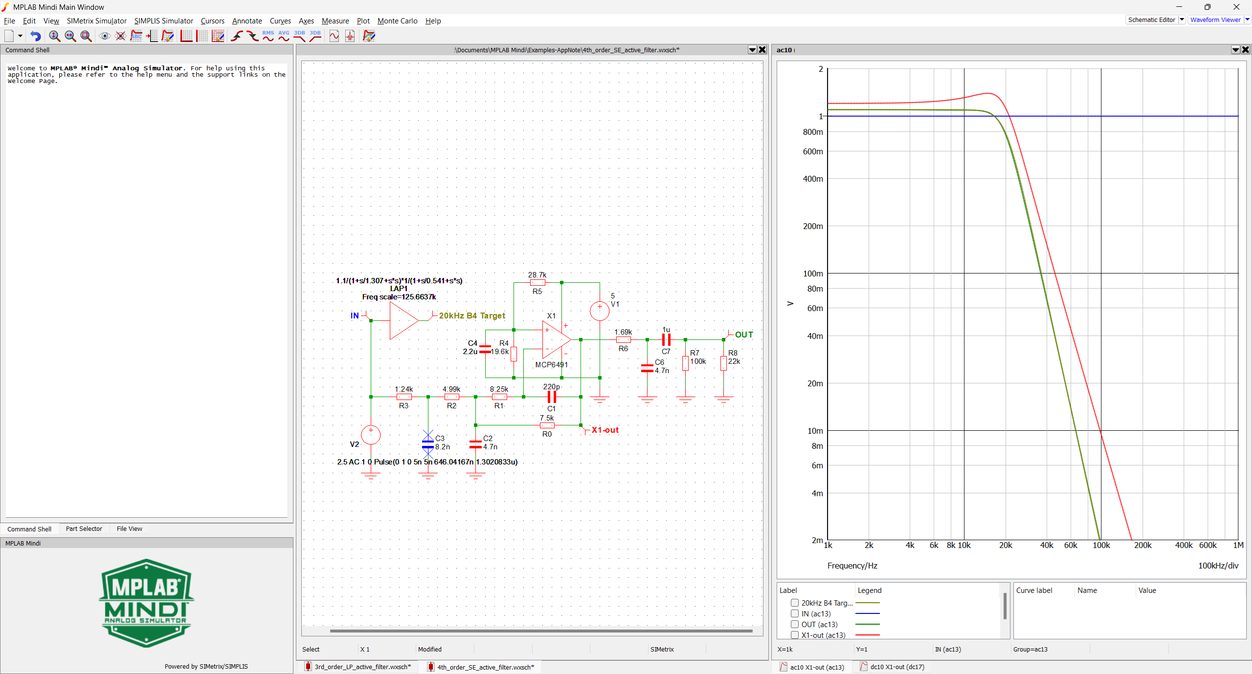
Changing C3 from 6.8 to 8.2 nF brings the simulated response to the B4 target.
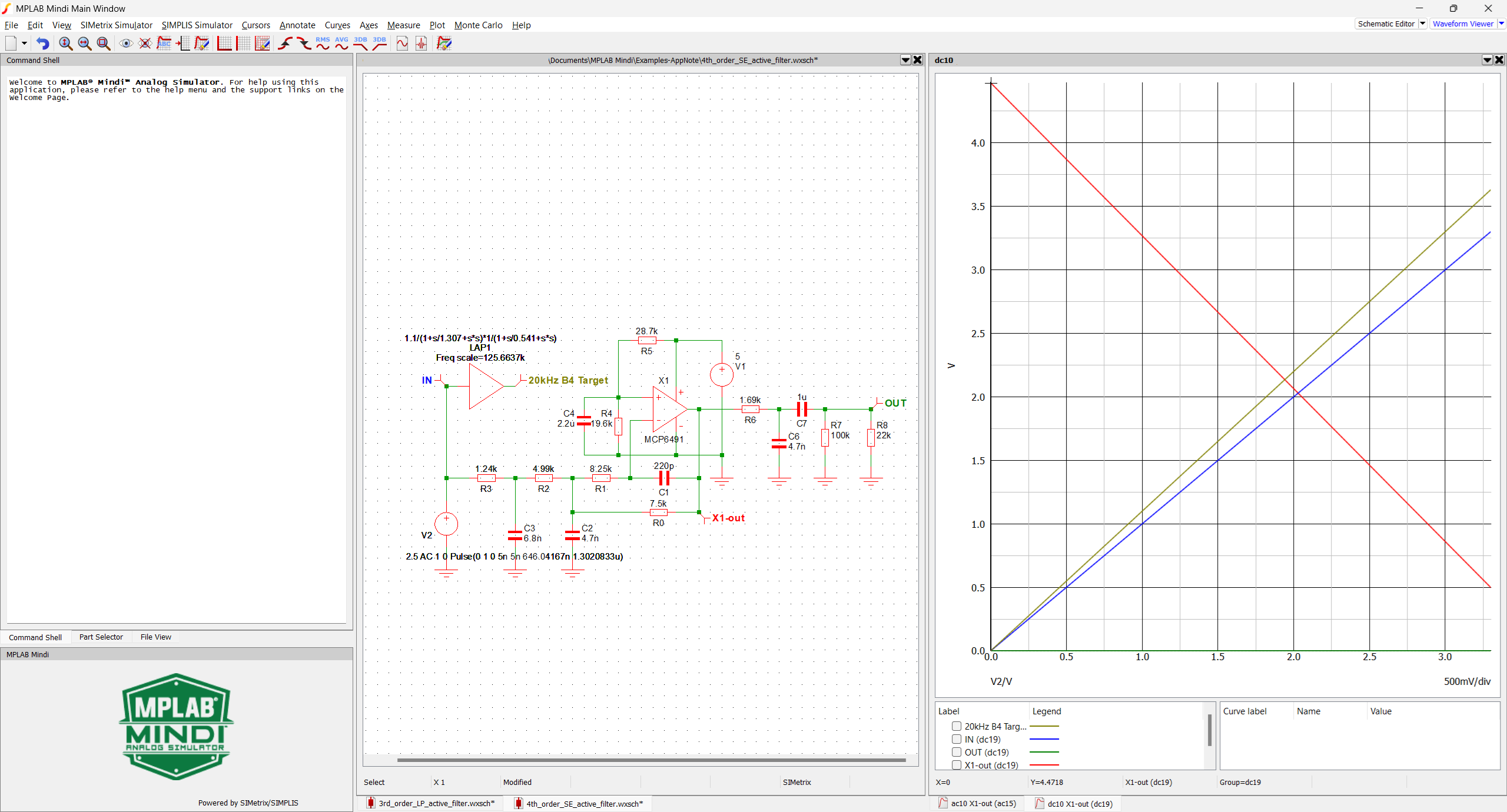
The DC simulation shows that applying the [0, 3.3V] input range (green curve) generates an output range close to [0.5, 4.5V] (red curve) at the amplifier output.
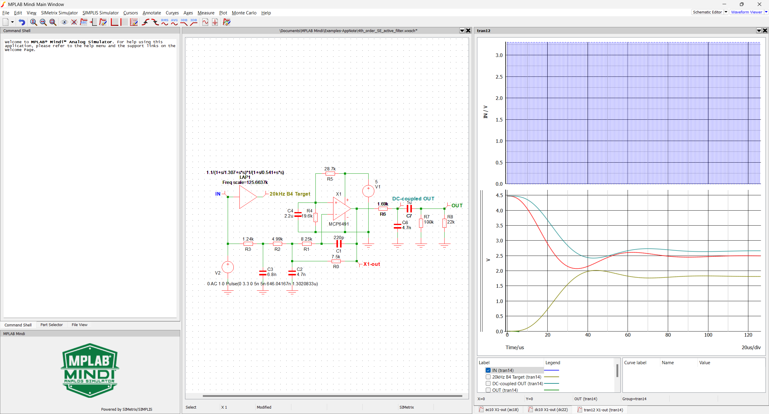
The transient simulation confirms the step response overshoot at the output of the amplifier (red trace). The step height in Steady state is 2V, very close to the expected 3.3V*50%*1.2. The overshoot adds 0.4V. Hence, the extra gain is 2.4/2=1.2, also very close to the predicted 1.18 value.