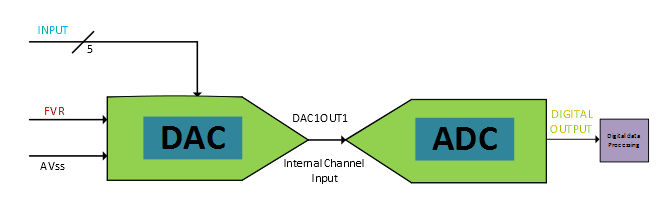
This particular configuration, useful for applications such as calibration,
involves two peripherals:
DAC for providing analog voltage to ADC channel
ADC for application functionalities
The user can configure the DAC output as input to ADC, the DAC positive
reference input as FVR buffer, the negative reference input source as microcontroller
GND (i.e., AVSS), and the DAC output routed to ADC as an input channel. The
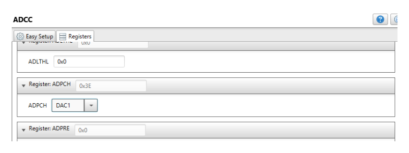
DAC output can be configured as an analog input channel to ADC by configuring the ADC
input selection register.
Figure 1-98. DAC Output as ADC Input
Configuration
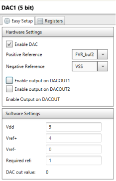
The DAC1CON0 resister must be configured as per requirements. Figure 4-5 shows code generation using MCC for the
DAC configuration.Figure 1-99. DAC Configuration for Reading
DAC Output Using ADC
The following code is generated by the MCC for the DAC configuration:
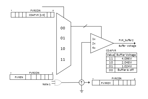
Figure 4-6 showcases the block diagram of FVR,
which can be used as a DAC positive reference input voltage. The FVRCON register is used
to set the fixed reference voltage for DAC.
Figure 1-100. FVR Configuration for DAC
Reference Voltage
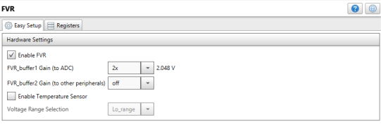
Figure 4-7 shows how the MCC can be used to generate the code
for FVR initialization. Figure 1-101. MCC Configuration to Set the
FVR Voltage as DAC Reference Voltage
The following code is generated by the MCC for the FVR
configuration:
The value of the ADPCH register for configuring the DAC output as an input
channel to ADC is 0b111110. Figure 4-8 shows the ADC module configuration to set the DAC
output as input to the ADC channel. Figure 1-102. MCC Configuration for
Selecting DAC as an ADC Input