
5.4 Ripple Injection
The VFB ripple required for proper operation of the MIC26400 gm amplifier and error comparator is 20mV to 100mV. However, the output voltage ripple is generally designed as 1% to 2% of the output voltage. For a low output voltage, such as 1V, the output voltage ripple is only 10mV to 20mV and the feedback voltage ripple is less than 20mV. If the feedback voltage ripple is so small that the gm amplifier and error comparator can’t sense it, the MIC26400 will lose control and the output voltage is not regulated. In order to have some amount of VFB ripple, a ripple injection method is applied for low output voltage ripple applications.
The applications are divided into three situations according to the amount of the feedback voltage ripple:
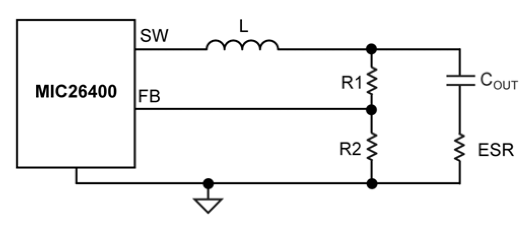
1) Enough ripple at the feedback voltage due to the large ESR of the output capacitors.
As shown in Figure 5-1, the converter is stable without any ripple injection. The feedback voltage ripple is:
Where:
ΔIL(PP) = The peak-to-peak value of the inductor current ripple.
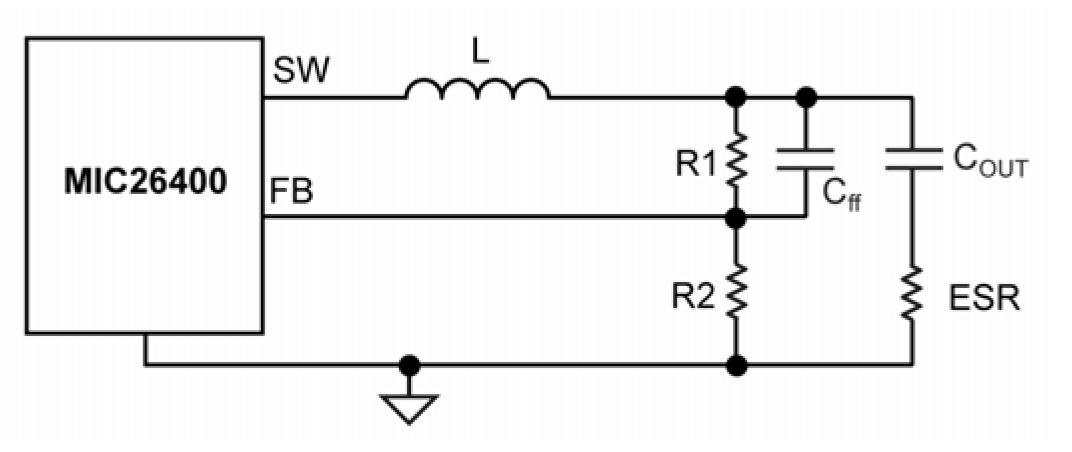
2) Inadequate ripple at the feedback voltage due to the small ESR of the output capacitors.
The output voltage ripple is fed into the FB pin through a feed-forward capacitor, CFF in this situation, as shown in Figure 5-2. The typical CFF value is between 1nF and 100nF.
With the feed-forward capacitor, the feedback voltage ripple is very close to the output voltage ripple:
3) Virtually no ripple at the FB pin voltage due to the very low ESR of the output capacitors.
In this situation, the output voltage ripple is less than 20mV. Therefore, additional ripple is injected into the FB pin from the switching node SW via a resistor RINJ and a capacitor CINJ, as shown in Figure 5-3. The injected ripple is:
Where:
VIN = The power stage input voltage.
D = Duty cycle.
fSW = Switching frequency.
τ = (R1//R2//RINJ) x CFF
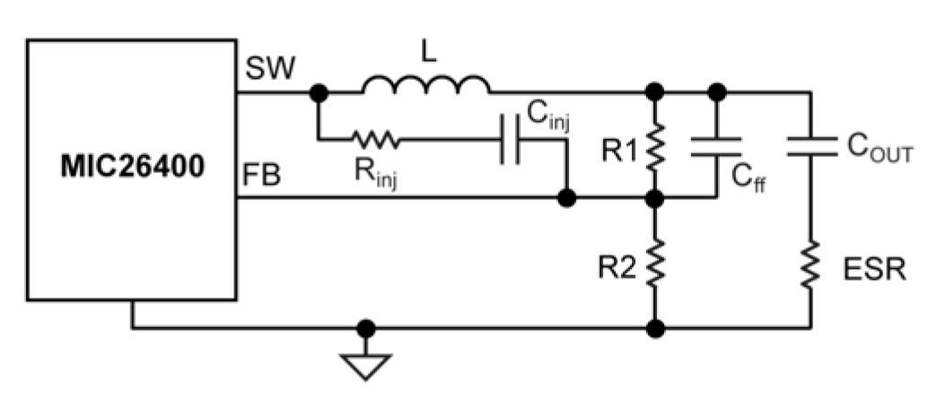
In the two previous equations, it is assumed that the time constant associated with CFF must be much greater than the switching period:
If the voltage divider resistors R1 and R2 are in the kΩ range, a CFF of 1nF to 100nF can easily satisfy the large time constant requirements. Also, a 100nF injection capacitor CINJ is used in order to be considered as short for a wide range of the frequencies.
The process of sizing the ripple injection resistor and capacitors is:
Step 1. Select CFF to feed all output ripples into the feedback pin and make sure the large time constant assumption is satisfied. Typical choice of CFF is 1nF to 100nF if R1 and R2 are in the kΩ range.
Step 2. Select RINJ according to the expected feedback voltage ripple using the following equations.
Then the value of RINJ is obtained using:
Step 3. Select CINJ as 100nF, which could be considered as short for a wide range of the frequencies.