
2.5.1 Invoking the Pin Planner
(Ask a Question)To invoke the Pin Planner, the design must be in the post-synthesis state.
- Invoke the Constraint Manager from the Design Flow window (Design Flow > Manage Constraints > Open Manage Constraints View).
- In the Constraints Manager, select the I/O Attributes tab and then select Edit > Edit with I/O Editor (I/O Attributes > Edit > Edit with I/O Editor). The I/O Editor opens.
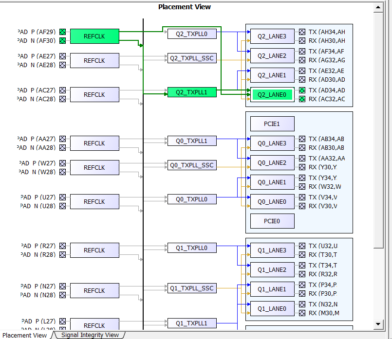
Placement View tab—Presents a physical view of the transceiver connectivity, including transceiver lanes (XCVR), Reference Clock (REFCLK), and Transmit PLLs (TxPLL).
Figure 2-32. IO Editor GUI 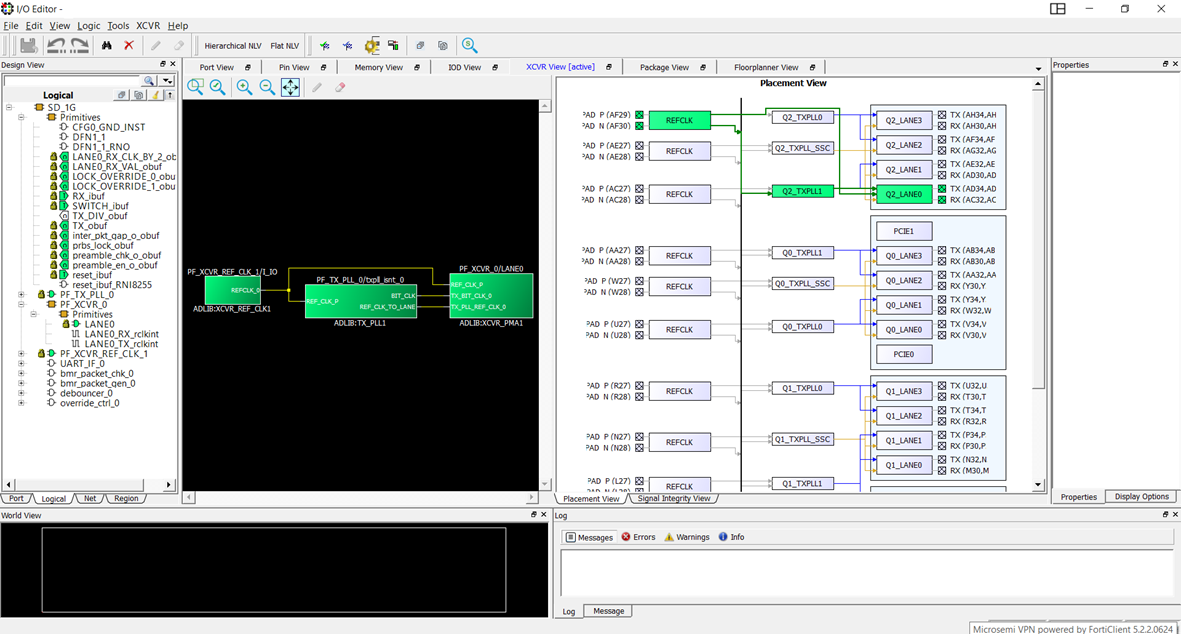
The transceiver view allows you to make assignments—XCVR, REFCLK, and TxPLLs. It has two views:
- A schematic view of the REFCLK, the TXPLL, and the XCVRs they drive.
- A graphical physical view of the REFCLK, its connection from the PADS to the TXPLL and the XCVR lanes.
The schematic and physical views provide design rule guidance for selecting legal connectivity combinations between the XCVR I/O, TxPLLs, and REFCLK inputs. It provides logical mapping to the device physical resources using connection rules of the device.
The following figure shows the XCVR Signal Integrity View tab. When user selects lane in Left Panel, the user can view and change the signal integrity parameters for the Rx and Tx transceiver ports.
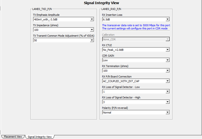
For more information about tuning the transceiver signal integrity, see Signal Integrity Conditioning.