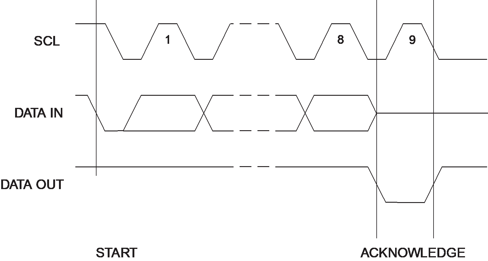
12.2 Timing Diagrams for Synchronous Communications
SCL: Serial Clock, SDA: Serial Data I/Op
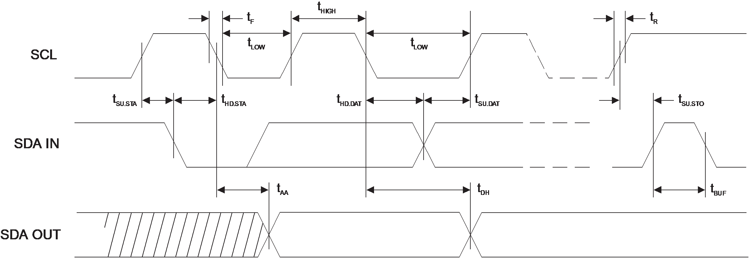
SCL: Serial Clock, SDA: Serial Data I/O
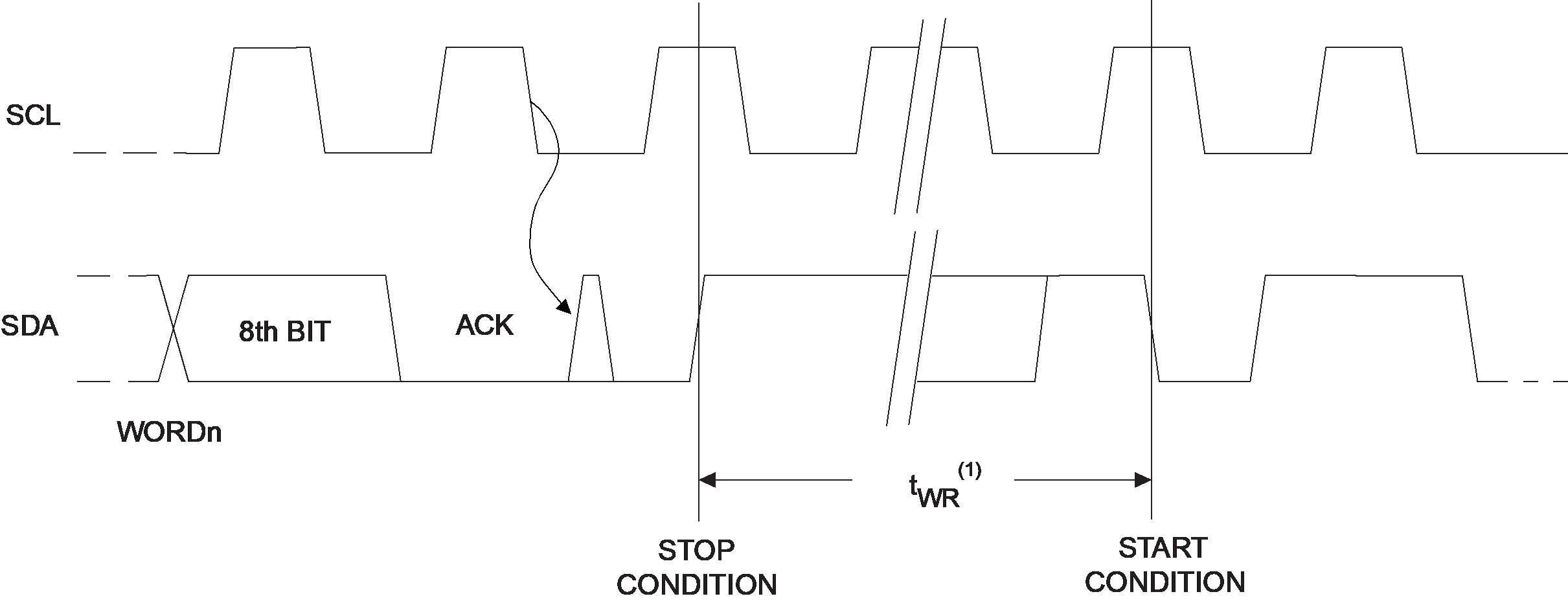
Note: The write cycle time tWR is the time from a valid
Stop condition of a write sequence to the end of the internal clear/write
cycle.