
47.4.3 Analog-to-Digital Converter (ADC) Characteristics
| Symbol | Parameters | Conditions | Min | Typ | Max | Unit |
|---|---|---|---|---|---|---|
| Res | Resolution | - | - | 12 | bits | |
| Rs | Sampling rate(2) | SAMPLEN = 3 resolution 12 bit (CTRLC.RESSEL = 0) | 10 | - | 1000 | ksps |
| Nb_cycles | Differential mode Number of ADC clock cycles SAMPCTRL.OFFCOMP = 1 | resolution 12 bit (CTRLC.RESSEL = 0) | - | 16 | - | cycles |
| resolution 10 bit (CTRLC.RESSEL = 2) | 14 | |||||
| resolution 8 bit (CTRLC.RESSEL = 3) | 12 | |||||
| Differential mode Number of ADC clock cycles SAMPCTRL.OFFCOMP = 0 SAMPLEN corresponds to the decimal value of SAMPCTRL.SAMPLEN[5:0] register | resolution 12 bit (CTRLC.RESSEL = 0) | - | SAMPLEN+13 | - | cycles | |
| resolution 10 bit (CTRLC.RESSEL = 2) | SAMPLEN+11 | |||||
| resolution 8 bit (CTRLC.RESSEL = 3) | SAMPLEN+9 | |||||
| Single-ended mode Number of ADC clock cycles SAMPCTRL.OFFCOMP = 1 | resolution 12 bit (CTRLC.RESSEL= 0) | - | 16 | - | cycles | |
| resolution 10 bit (CTRLC.RESSEL= 2) | 15 | |||||
| resolution 8 bit (CTRLC.RESSEL= 3) | 13 | |||||
| Single-ended mode Number of ADC clock cycles SAMPCTRL.OFFCOMP = 0 SAMPLEN corresponds to the decimal value of SAMPCTRL.SAMPLEN[5:0] register | resolution 12 bit (CTRLC.RESSEL= 0) | - | SAMPLEN+13 | - | cycles | |
| resolution 10 bit (CTRLC.RESSEL= 2) | SAMPLEN+12 | |||||
| resolution 8 bit (CTRLC.RESSEL= 3) | SAMPLEN+10 | |||||
| fadc | ADC Clock frequency | 160 | - | 16000 | kHz | |
| Ts | Sampling time | SAMPCTRL.OFFCOMP = 1 | 250 | - | 25000 | ns |
| SAMPCTRL.OFFCOMP = 0 | (SAMPLEN+1)/fadc | - | - | s | ||
| Sampling time with DAC as input | - | 3 | - | - | µs | |
| Sampling time with Bandgap as input | - | 10 | - | - | µs | |
| Vcnv | Conversion range | Differential mode | -VREF | - | +VREF | V |
| Single-ended mode | 0 | - | VREF | |||
| Vref | Reference input | - | 2 | - | VDDANA-0.6 | V |
| Vin | Input channel range | - | 0 | - | VDDANA | V |
| Vcmin | Input common mode voltage | CTRLC.R2R = 1 | 0.2 | - | VREF-0.2 | V |
| CTRLC.R2R = 0 | VREF/2-0.2 | - | VREF/2+0.2 | V | ||
| CSAMPLE | Input sampling capacitance | - | - | 3.2 | pF | |
| RSAMPLE | Input sampling on-resistance | For a sampling rate at 1 Msps | - | 1000 | 1715 | Ω |
| Rref | Reference input source resistance | 0 | - | 1000 | kΩ |
Note:
- These values are based on simulation. These values are not covered by test limits in production or characterization.
- Sampling rate (in samples per second) is equal to Nb_cycles/fadc.
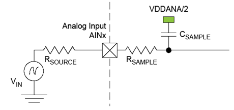
The minimum sampling time tsamplehold for a given Rsource can be found using this formula:
For 12-bit accuracy:
| Symbol | Parameter | Conditions | Measurement | Unit | |||
|---|---|---|---|---|---|---|---|
| Min | Typ | Max | |||||
| ENOB(1) | Effective Number of bits | Fadc = 500 ksps - R2R disabled | Vddana = 5.0V Vref = Vddana | 9.9 | 10.7 | 11.4 | bits |
| Vddana = 2.7V Vref = 2.0V | 10.0 | 10.8 | 11.3 | ||||
| Fadc = 1 Msps - R2R disabled | Vddana = 5.0V Vref = Vddana | 9.7 | 10.6 | 11.3 | |||
| Vddana = 2.7V Vref = 2.0V | 9.8 | 10.6 | 11.2 | ||||
| Fadc = 500 ksps - R2R Enabled(2) | Vddana = 5.0V Vref = Vddana | 9.8 | 11.3 | 11.9 | |||
| Fadc = 1 Msps - R2R Enabled(2) | Vddana = 5.0V Vref = Vddana | 9.7 | 11.1 | 11.8 | |||
| TUE | Total Unadjusted Error | Fadc = 500 ksps - R2R disabled with offset and gain
compensation (REFCOMP = 1 and OFFCOMP = 1) | Vddana = 5.0V Vref = Vddana | - | +/-3.4 | +/-5 | LSB |
| Vddana = 2.7V Vref = 2.0V | - | +/-3 | +/-5.6 | ||||
| Fadc = 1 Msps - R2R disabled with offset and gain
compensation (REFCOMP = 1 and OFFCOMP = 1) | Vddana = 5.0V Vref = Vddana | - | +/-4.2 | +/-6.3 | |||
| Vddana = 2.7V Vref = 2.0V | - | +/-3.6 | +/-7.7 | ||||
| INL | Integral Non Linearity | Fadc = 500 ksps - R2R disabled | Vddana = 5.0V Vref = Vddana | - | +/-1.9 | +/-3.5 | LSB |
| Vddana = 2.7V Vref = 2.0V | - | +/-1.6 | +/-3.5 | ||||
| Fadc = 1 Msps - R2R disabled | Vddana = 5.0V Vref = Vddana | - | +/-2 | +/-3.3 | |||
| Vddana = 2.7V Vref = 2.0V | - | +/-1.9 | +/-3.6 | ||||
| DNL | Differential Non Linearity | Fadc = 500 ksps - R2R disabled | Vddana = 5.0V Vref = Vddana | - | -0.9/+1 | -1/+1.2 | LSB |
| Vddana = 2.7V Vref = 2.0V | - | -0.9/+1.1 | -1/+2.1 | ||||
| Fadc = 1 Msps - R2R disabled | Vddana = 5.0V Vref = Vddana | - | -0.9/+1 | -1/+1 | |||
| Vddana = 2.7V Vref = 2.0V | - | -1/+1.6 | -1/+3.6 | ||||
| GE | Gain Error | Fadc = 1 Msps - R2R disabled w/o gain compensation | Vddana = 5.0V Vref = Vddana | - | +/-0.06 | +/-0.3 | % |
| Vddana = 2.7V Vref = 2.0V | - | +/-0.06 | +/-1.2 | ||||
| Vddana = 5.0V 1V internal Ref | - | +/-1.9 | +/-6.5 | ||||
| Vddana = 5.0V Vref = Vddana/2 | - | +/-0.11 | +/-0.82 | ||||
| Fadc = 1 Msps - R2R disabled with gain compensation | Vddana = 2.7V Vref = 2.0V | - | +/-0.03 | +/-0.46 | |||
| Vddana = 5.0V Vref = Vddana/2 | - | +/-0.13 | +/-0.58 | ||||
| OE | Offset Error | Fadc = 1 Msps - R2R disabled without offset compensation | Vddana = 5.0V Vref = Vddana/2 | - | +/-0.8 | +/-13 | mV |
| Vddana = 2.7V Vref = 2.0V | - | +/-0.7 | +/-9.7 | ||||
| Fadc = 1 Msps - R2R disabled with offset compensation | Vddana = 5.0V Vref = Vddana/2 | - | +/-0.01 | +/-5.6 | |||
| Vddana = 2.7V Vref = 2.0V | - | +/-0.4 | +/-4.2 | ||||
| SFDR | Spurious Free Dynamic Range | Fs = 1Msps / Fin = 14 kHz / Full range Input signal Vddana = 5.0V Vref = Vddana | 63 | 71 | 81 | dB | |
| SINAD(1) | Signal to Noise and Distortion ratio | 60 | 65 | 70 | |||
| SNR at -3 db FS | Signal to Noise ratio | 64 | 67 | 70 | |||
| THD | Total Harmonic Distortion | 63 | -70 | 81 | |||
| Noise RMS | External Reference voltage | - | 0.4 | 3.2 | mV | ||
- Referred to Full Scale.
- Dynamical input range is +/-6% of Full scale.
| Symbol | Parameter | Conditions | Measurement | Unit | |||
|---|---|---|---|---|---|---|---|
| Min | Typ | Max | |||||
| ENOB(1) | Effective Number of bits | Fadc = 500 ksps - R2R disabled | Vddana = 3.0V Vref = Vddana | 9.0 | 9.7 | 10.2 | bits |
| Vddana = 3.0V Vref = 2.0V | 9.0 | 9.6 | 10.1 | ||||
| Fadc = 1 Msps - R2R disabled | Vddana = 3.0V Vref = Vddana | 8.9 | 9.6 | 10.0 | |||
| Vddana = 3.0V Vref = 2.0V | 8.9 | 9.4 | 9.7 | ||||
| TUE | Total Unadjusted Error | Fadc = 500 ksps - R2R disabled with offset and gain
compensation (REFCOMP = 1 and OFFCOMP = 1) | Vddana = 5.0V Vref = Vddana | - | +/-12.9 | +/-25.2 | LSB |
| Vddana = 2.7V Vref = 2.0V | - | +/-25 | +/-49.6 | ||||
| Fadc = 1 Msps - R2R disabled with offset and gain
compensation (REFCOMP = 1 and OFFCOMP = 1) | Vddana = 5.0V Vref = Vddana | - | +/-13.5 | +/-26.4 | |||
| Vddana = 2.7V Vref = 2.0V | - | +/-27 | +/-52 | ||||
| INL | Integral Non Linearity | Fadc = 500 ksps - R2R disabled | Vddana = 5.0V Vref = Vddana | - | +/-3.7 | +/-6.5 | |
| Vddana = 2.7V Vref = 2.0V | - | +/-3.4 | +/-5.9 | ||||
| Fadc = 1 Msps - R2R disabled | Vddana = 5.0V Vref = Vddana | - | +/-4.2 | +/-7.4 | LSB | ||
| Vddana = 2.7V Vref = 2.0V | - | +/-3.5 | +/-6.2 | ||||
| DNL | Differential Non Linearity | Fadc = 500 ksps - R2R disabled | Vddana = 5.0V Vref = Vddana | - | -0.9/+1.2 | -1/+1.6 | |
| Vddana = 2.7V Vref = 2.0V | - | -0.9/+1.3 | -1/+2.3 | ||||
| Fadc = 1 Msps - R2R disabled | Vddana = 5.0V Vref = Vddana | - | -1/+1.1 | -1/+1.3 | |||
| Vddana = 2.7V Vref = 2.0V | - | -1/+1.4 | -1/+3.1 | ||||
| GE | Gain Error | Fadc = 1 Msps - R2R disabled w/o gain compensation | Vddana = 5.0V Vref = Vddana | - | +/-0.2 | +/-0.7 | % |
| Vddana = 2.7V Vref = 2.0V | - | +/-0.3 | +/-1.4 | ||||
| Vddana = 5.0V 1V internal Ref | - | +/-1.6 | +/-6.6 | ||||
| Vddana = 5.0V Vref = Vddana/2 | - | +/-0.2 | +/-1.1 | ||||
| Fadc = 1 Msps - R2R disabled with gain compensation | Vddana = 2.7V Vref = 2.0V | - | +/-0.3 | +/-0.8 | |||
| Vddana = 5.0V Vref = Vddana/2 | - | +/-0.1 | +/-0.5 | ||||
| OE | Offset Error | Fadc = 1 Msps - R2R disabled | Vddana = 5.0V Vref = Vddana | - | +/-7 | +/-63 | mV |
| Vddana = 2.7V Vref = 2.0V | - | +/-7 | +/-64 | ||||
| SFDR | Spurious Free Dynamic Range | Fs = 1Msps / Fin = 14 kHz / Full range Input signal Vddana = 5.0V Vref = Vddana | 57 | 66 | 73 | dB | |
| SINAD(1) | Signal to Noise and Distortion ratio | 54 | 59 | 62 | |||
| SNR at -3 db FS | Signal to Noise ratio | 57 | 60 | 62 | |||
| THD | Total Harmonic Distortion | -71 | -64 | -56 | |||
| Noise RMS | External Reference voltage | - | 0.6 | 1.9 | mV | ||
- Referred to Full Scale.