
2 PCIe MSS
(Ask a Question)The PolarFire® SoC FPGA PCIe block connects to the MSS LPDDR4 and LSRAM block through MSS Fabric Interface Controllers (FIC0) AXI4 master bus interface. The PCIe AXI_1_Master is interconnected with CoreAXI4Interconnect bus, and this is configured for single master and two slaves. It is used to connect the PF_PCIE_C0_0 with PCIe LSRAM and MSS LPDDR4 for DMA operations. The PF_PCIE_C0_0 IP block is used to configure the PCIESS as a Root Port (PCIe 1). PCIESS block is configured for x4 lanes, 5 Gbps data-rate, and APB interface for PCIe Controller access. Root port system uses Dynamic Reconfiguration Interface (DRI) to access the PCIe and PCS soft reset registers. The APB3 interface is enabled to access the PCIe DMA and address translation registers. Interrupt (IRQ) MSS_INT_F2M[1] is mapped to PCIE_1_INTERRUPT_OUT of PF_PCIE_C0_0. The PolarFire SoC FPGA on one board is programmed with the PCIe Root Port design and the PolarFire FPGA on the other board is programmed with the PCIe Endpoint design.
The PolarFire PCIe Root Port can establish a PCIe link with any PCIe Endpoint or Bridge. The user application enumerates the Endpoint device using the Enhanced Configuration Access Mechanism (ECAM) feature. The user application also initiates the AXI transactions from the Root Port. These AXI transactions are converted to PCIe Configuration space or memory transactions (CfgWr/CfgRd/MWr/MRd) to Endpoint.
The top-level block diagram of the PCIe Root Port design is shown in the following figure.

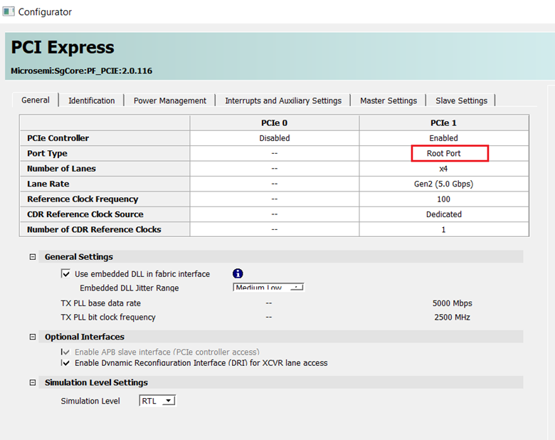
The following figure shows the PCIe IP configurator settings for PCIe Root Port in PolarFire SoC FPGA.
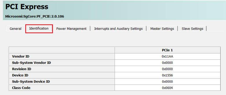
The following figure shows the Identification tab in the PCI Express configurator.
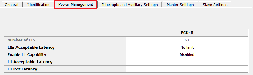
The following figure shows the Power Management tab in the PCI Express configurator.
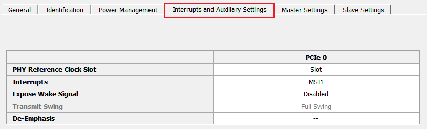
The following figure shows the Interrupts and Auxiliary Settings tab in the PCI Express configurator.
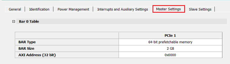
The following figure shows the Master Settings tab in the PCI Express configurator.
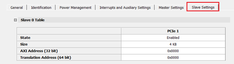
The following figure shows the Slave Settings tab in the PCI Express configurator.
References
- For information about DRI, see PolarFire Family DRI User Guide.
- For information about PolarFire SoC PCIe Root Port Linux reference design, see GitHub.
- For information about PolarFire SoC HSS, see GitHub.
- For information about Yocto BSP, see GitHub.