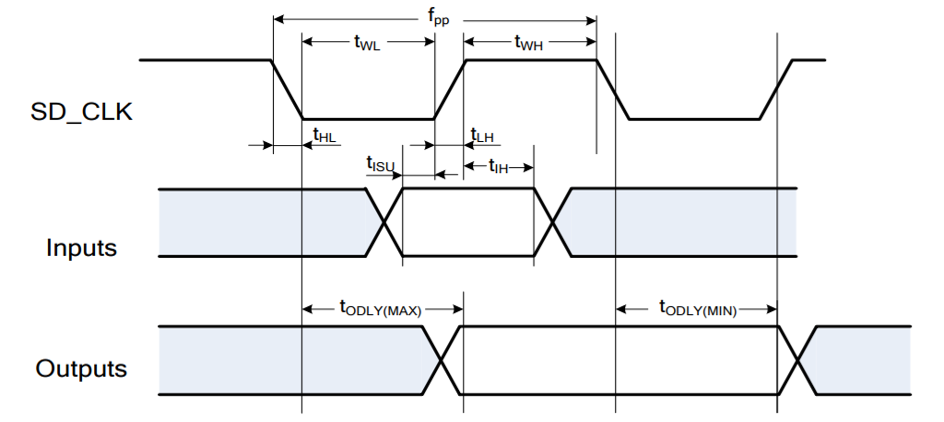
The SDIO Client interface timing for ATWILC3000A is
shown in the following figure.Figure 9-3. SDIO Client Timing Diagram
The following table provides the SDIO Client timing parameters for the ATWILC3000A.
Table 9-10. SDIO Client Timing Parameters
Parameter
Symbol
Min.
Max.
Units
Clock Input Frequency(1)
fPP
—
50
MHz
Clock Low Pulse Width
tWL
6
—
ns
Clock High Pulse Width
tWH
7
—
Clock Rise Time
tLH
0
5
Clock Fall Time
tHL
0
5
Input Setup Time
tISU
6
—
Input Hold Time
tIH
8
—
Output Delay(2)
tODLY
3
11
Note:
Maximum clock frequency specified is
limited by the SDIO Client interface internal design; actual maximum clock frequency can
be lower and depends on the specific PCB layout.
Timing based on 15 pF output
loading.
The online versions of the documents are provided as a courtesy. Verify all content and data in the device’s PDF documentation found on the device product page.