
4.1 Theory of Operation
The Functional Block Diagram illustrates the control loop of the MIC26400. The output voltage is sensed by the MIC26400 feedback pin FB via the voltage divider R1 and R2, and compared to a 0.8V reference voltage, VREF, at the error comparator through a low gain transconductance (gm) amplifier. If the feedback voltage decreases and the output of the gm amplifier is below 0.8V, then the error comparator will trigger the control logic and generate an ON-time period. The ON-time period length is predetermined by the “FIXED tON ESTIMATION” circuitry in the block diagram:
Where:
VOUT = The output voltage.
VIN = The power stage input voltage.
At the end of the ON-time period, the internal high-side driver turns off the high-side MOSFET and the low-side driver turns on the low-side MOSFET. The OFF-time period length depends upon the feedback voltage, in most cases. When the feedback voltage decreases and the output of the gm amplifier is below 0.8V, the ON-time period is triggered and the OFF-time period ends. If the OFF-time period determined by the feedback voltage is less than the minimum OFF-time tOFF(MIN), which is about 360ns, the MIC26400 control logic will apply the tOFF(MIN) instead. tOFF(MIN) is required to maintain enough energy in the boost capacitor (CBST) to drive the high-side MOSFET. The maximum duty cycle is obtained from the 360ns tOFF(MIN):
Where:
tS = 1/300kHz = 3.33µs.
Microchip does not recommend using MIC26400 with an OFF-time close to tOFF(MIN) during steady-state operation. Also, as VOUT increases, the internal ripple injection will increase and reduce the line regulation performance. Therefore, the maximum output voltage of the MIC26400 should be limited to 5.5V. Please refer to the Setting Output Voltage section for more details.
The actual ON-time and resulting switching frequency will vary with the part-to-part variation in the rise and fall times of the internal MOSFETs, the output load current, and variations in the VDD voltage. Also, the minimum tON results in a lower switching frequency in high VIN to VOUT applications, such as 26V to 1.0V. The minimum tON measured on the MIC26400 evaluation board is about 184ns. During load transients, the switching frequency is changed due to the varying OFF-time.
To illustrate the control loop operation, we will analyze both the steady-state and load transient scenarios. For easy analysis, the gain of the gm amplifier is assumed to be 1. With this assumption, the inverting input of the error comparator is the same as the feedback voltage.
Figure 4-1 shows the MIC26400 control loop timing during steady-state operation. During steady-state, the gm amplifier senses the feedback voltage ripple, which is proportional to the output voltage ripple and the inductor current ripple, to trigger the ON-time period. The ON-time is predetermined by the tON estimator. The termination of the OFF-time is controlled by the feedback voltage. At the valley of the feedback voltage ripple, which occurs when VFB falls below VREF, the OFF period ends and the next ON-time period is triggered through the control logic circuitry.
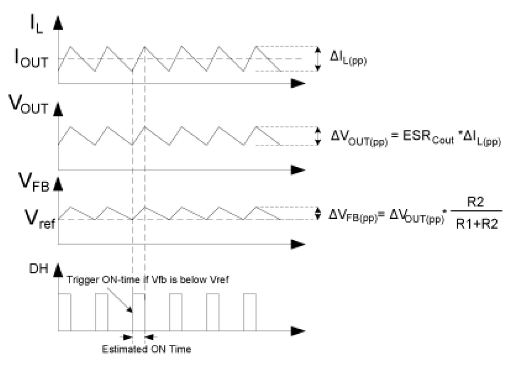
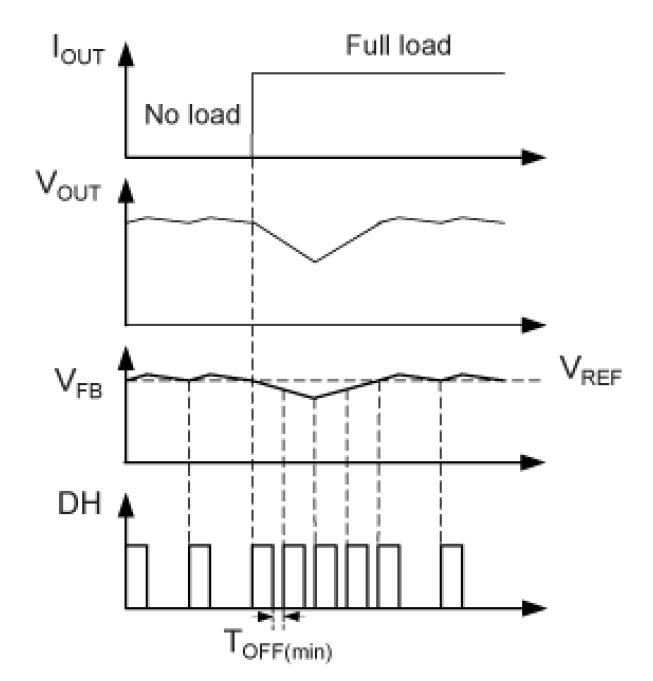
Figure 4-2 shows the operation of the MIC26400 during a load transient. The output voltage drops due to the sudden load increase, which causes VFB to be less than VREF. This will cause the error comparator to trigger an ON-time period. At the end of the ON-time period, a minimum OFF-time, tOFF(MIN), is generated to charge CBST because the feedback voltage is still below VREF. Then, the next ON-time period is triggered due to the low feedback voltage. Therefore, the switching frequency changes during the load transient, but returns to the nominal fixed frequency once the output has stabilized at the new load current level. With the varying duty cycle and switching frequency, the output recovery time is fast and the output voltage deviation is small in MIC26400 converter.
Unlike true current-mode control, the MIC26400 uses the output voltage ripple to trigger an ON-time period. The output voltage ripple is proportional to the inductor current ripple if the ESR of the output capacitor is large enough. The MIC26400 control loop has the advantage of eliminating the need for slope compensation.
In order to meet the stability requirements, the MIC26400 feedback voltage ripple should be in phase with the inductor current ripple and large enough to be sensed by the gm amplifier and the error comparator. The recommended feedback voltage ripple is 20mV~100mV. If a low-ESR output capacitor is selected, the feedback voltage ripple may be too small to be sensed by the gm amplifier and the error comparator. Also, the output voltage ripple and the feedback voltage ripple are not necessarily in phase with the inductor current ripple if the ESR of the output capacitor is very low. In these cases, ripple injection is required to ensure proper operation. Please refer to the Ripple Injection section for more details about the ripple injection technique.