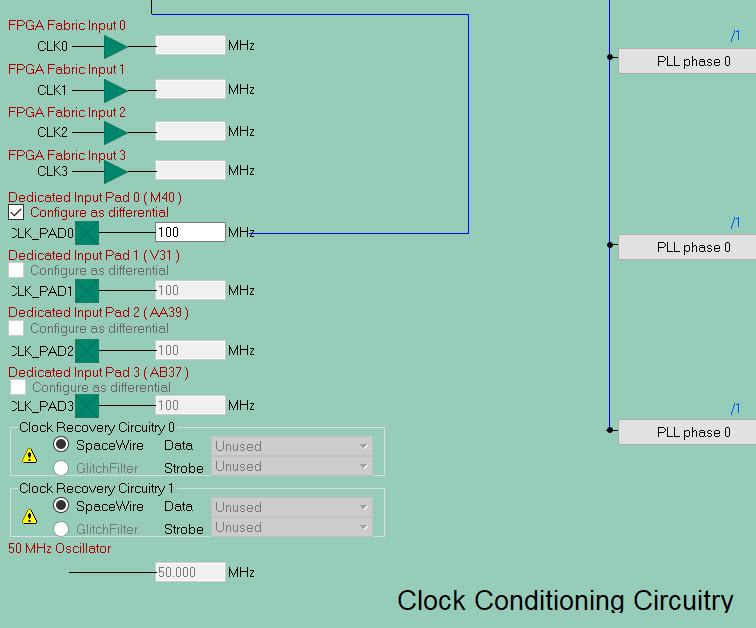
2.4.2.5 Input Clocks Configuration
You must enter the clock frequency of each CCC input used in the configuration as the PLL reference clock, PLL feedback clock, or Output direct connection. These frequencies are used to compute the PLL configuration and divider configuration that meet the output frequencies requirements.
Use Clock Recovery Circuitry to configure the CCC outputs to connect to Spacewire or Glitch Filter.
The following figure shows the DRCs reported. The dedicated input pad[#] frequency must be less than 400 MHz.

Dedicated Input Pad
Some of the dedicated inputs to the CCC can be configured to use a differential I/O technology. The location, I/O technology and attributes available for each CCC dedicated input pad is described in the RTG4 FPGA Datasheet.Clock Recovery Circuitry
Each CCC block has two dedicated Clock Recovery Circuitry blocks: Block 0 and Block 1. These can be used in either the SpaceWire mode (Default) or the Glitch Filter mode.
The RX clock is based on Data and Strobe Inputs, which are from external dedicated I/Os. The Clock Recovery Circuitry Blocks also include a de-glitching circuit to prevent any undesirable narrow clock pulse at output.
- You can select the Dedicated input pad 1 and 3 for Data signal. Dedicated input pads 0 and 2 are automatically set as corresponding Strobe signal.
- The same pair of Dedicated input pads cannot be simultaneously used in Clock Recovery Circuitry.
- Dedicated input pads, which are used as Data and Strobe signals for Clock Recovery Circuitry block cannot be used as input to PLL Reference Clock and PLL Feedback Clock.
- You cannot set input frequency values for Dedicated pads, which are configured as Data and Strobe signals for RX Clock Recovery Circuitry.
- Clock Recovery Circuitry Block 0 and 1 cannot have the same input source when both are configured for SpaceWire mode.
- Clock Recovery Circuitry Block 0 and 1 cannot have the same input source when both are configured for Glitch Filter mode.
- Clock Recovery Circuitry Block 0 and 1 cannot have the same input source when one is configured for SpaceWire mode and the other is configured for Glitch Filter mode.
- It is valid to select the same input for PLL REFCLK (and CGL secondary clock) and Glitch Filter.
