
42.4.5 Reset, WDT, Power-up Timer, and Brown-Out Reset Specifications
Note:
- Asserted low.
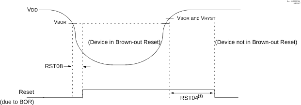
Note:
- Only if
PWRTE bit in the Configuration Word register is
programmed to ‘
1’; 2 ms delay if PWRTE =0.
| Standard Operating Conditions (unless otherwise stated) | |||||||
|---|---|---|---|---|---|---|---|
| Param No. | Sym. | Characteristic | Min. | Typ. † | Max. | Units | Conditions |
| RST01* | TMCLR | MCLR Pulse Width Low to ensure Reset | — | 0.6 | — | μs | |
| RST02* | TIOZ | I/O high-impedance from Reset detection | — | — | 2.0 | μs | |
| RST03* | TWDT | Watchdog Timer Time-out Period | — | 16.0 | — | ms | WDTCPS = 'b00100 |
| RST04* | TPWRT | Power-up Timer Period | — | 65.0 | — | ms | PWRTS = 'b10 |
| RST05* | TOST | Oscillator Start-up Timer Period(1,2) | — | 1024 | — | TOSC | |
| RST06 | VBOR | Brown-out Reset Voltage | 2.50 | 2.65 | 2.80 | V | BORV =0 |
| RST06A | 1.80 | 1.90 | 2.05 | V | BORV = 1 | ||
| RST07* | VBORHYS | Brown-out Reset Hysteresis | — | 35.0 | — | mV | BORV = 0 |
| RST08* | TBORDC | Brown-out Reset Response Time | — | 3.0 | — | μs | |
| RST09 | VLPBOR | Low-Power Brown-out Reset Voltage | 1.80 | 1.90 | 2.40 | V | |
| RST09A* | VLPBORHYS | Low-Power Brown-out Hysteresis | — | 25.0 | — | mV | |
|
* These parameters are characterized but not tested. † Data in “Typ” column is at 3.0V, 25°C unless otherwise stated. These parameters are for design guidance only and are not tested. Note:
| |||||||