
14.5.6 Programming Flash Pages
Page programming into the internal Flash uses a page cache in internal SRAM0 to speed up to the process, writing all page data at once in the internal Flash.
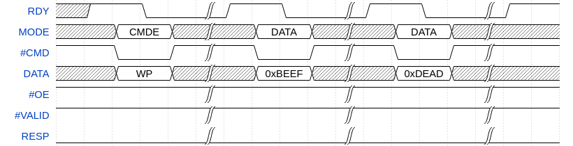
The above example shows how to write the [0xEF, 0xBE, 0xAD, 0xDE] byte sequence into the page cache. Since Flash pages are 512 bytes, the offset in the page cache where any 16-bit data is written is given by current value ADDR[8:0] before the auto increment. In turn, the page index where the page cache will be flushed into is given in ADDR[31:9]. A value of zero for page index makes the address parameter point to the very first page of the internal Flash.
At the end of a DATA command, if the auto increment of ADDR[31:0] crosses the page boundary, then a page cache flush into the internal Flash is automatically triggered at the beginning of the next DATA command, before writing the new data into the page cache. If no more data are to be written, a page cache flush can be manually triggered by sending a CMDE command, similar to a simple SYNC operation.
Before executing a DATA command during a Write Page operation (WP, EWP, WPL, EWPL)s, the ADDR[31:0] register should always be aligned to 2 bytes, meaning ADDR[0] = 0.
If an error occurs while flushing the page cache, the FPPI Monitor raises the RESP line:
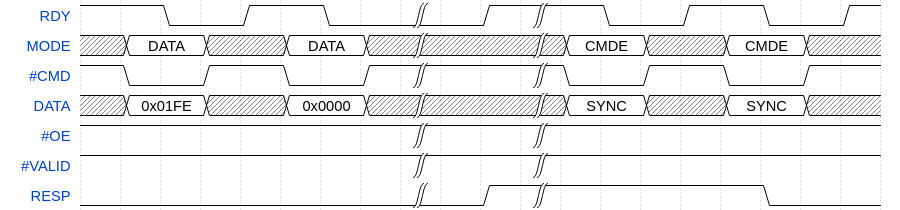
In the above example, the sequence of bytes [0xFE, 0x01, 0x00, 0x00] is written into the page cache. The page boundary is crossed after byte 0x01 so the 2nd DATA command triggers a page cache flush. This flush operation fails, so the FFPI Monitor raises the RESP line. Later the host sends two CMDE commands to acknowledge the error so the FFPI Monitor lowers the RESP line.