
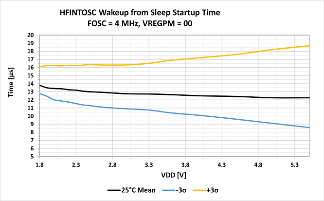
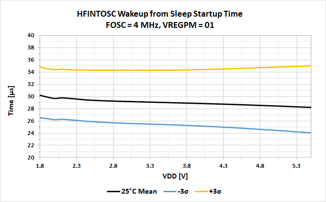
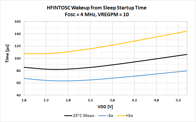
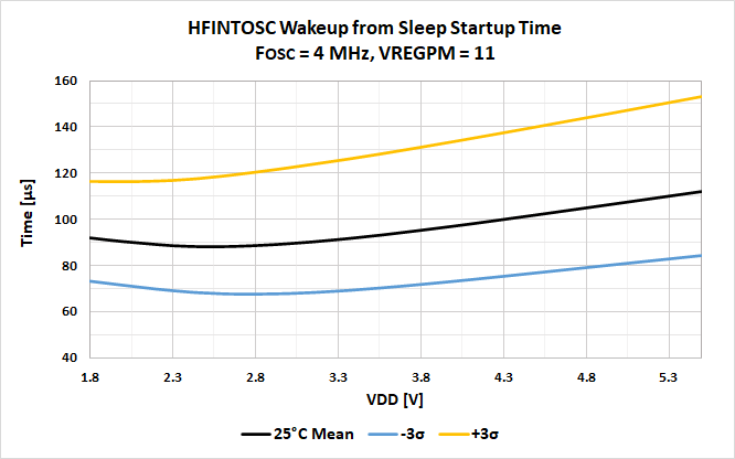
51.6 HFINTOSC Wake From Sleep Graphs
| 
|
| 
|
|
|
|
|
|
|
The online versions of the documents are provided as a courtesy. Verify all content and data in the device’s PDF documentation found on the device product page.