Clock signals are routed
differentially, and the length matches between traces should be ±5 mils.
It should be referenced to ground plane.
The space between clock and other
signals must be 25 mils.
One clock signal is routed per
rank of the Dual Inline Memory Module (DIMM), that is, one clock for
single-ranked DIMM, two clock signals for the dual ranked DIMM. For non-DIMM
systems, the differential terminations used by the CK/CK# pair must be located
as close as possible to the memory.
If more than one CS is used, the
same clock to DQS skew must be applied to all CS.
Address/control signals and the associated CK and CK# differential FPGA clock
should be routed with trace matching ±100 mil.
Note: The following guidelines are applicable for DDR2, DDR3, and LPDDR:
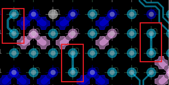
Short the MDDR_TMATCH_0_IN and MDDR_TMATCH_0_OUT pins under BGA using short
trace.
Short the MDDR_TMATCH_1_IN and MDDR_TMATCH_1_OUT pins under BGA using short
trace.
Short the MDDR_TMATCH_ECC_IN and MDDR_TMATCH_ECC_OUT pins under BGA using
short trace.
Short the FDDR_TMATCH_0_IN and FDDR_TMATCH_0_OUT pins under BGA using short
trace.
Short the FDDR_TMATCH_1_IN and FDDR_TMATCH_1_OUT pins under BGA using short
trace.
Short the FDDR_TMATCH_ECC_IN and FDDR_TMATCH_ECC_OUT pins under BGA using
short trace.
For more information about DDR2 and LPDDR memory layout guidelines, see
the Micron Memory Layout Guidelines in the following documents, available on the
Micron website:
TN-47-20: Hardware Tips for Point-to-Point System Design from Micron
TN-46-19: Hardware Tips for Point-to-Point System Design from Micron
The following figure shows an example layout. Figure 2-39. TMATCH Signals (Example Layout)
The online versions of the documents are provided as a courtesy. Verify all content and data in the device’s PDF documentation found on the device product page.