
2.5.2 Plane Layout
(Ask a Question)- Plane routing for PLL0VDDA and PLL0VSSA is shown in the following figure. These are with respect to the schematic, as shown in Figure 2-17.
- The capacitor (22 μF) and series resistor
must be placed close to the device to the 0.1 μF capacitor. A sample placement is shown in
the following figure.
Figure 2-19. Routing for PLL Filter Circuit 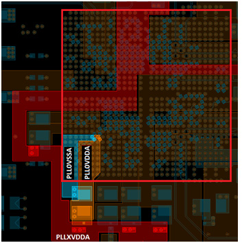
PLL0VDDA and PLL0VSSA must not be routed with a small trace width as it increases the inductance resulting in ripples. These supply traces must be routed as plane (as shown in Figure 2-19), even though the current requirements are small.
Same layout guidelines must be followed for DDR PLL power supplies. For more information about PCIe PLL guidelines, see SerDes.