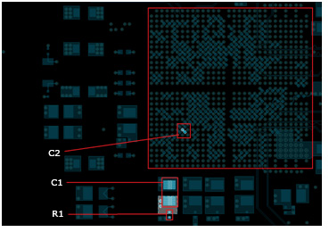
The capacitor (C1) and series resistor (R1)
must be placed near the device as close as possible to C2 device. A sample placement is
shown in the following figure.
The decoupling capacitor (C2) must be
placed near the BGA via. The capacitor pad to via trace must be small. For more information
about R1, C1, and C2, see Design Considerations.
Figure 2-18. Placement of Capacitors for PLL Filter
Circuit
The online versions of the documents are provided as a courtesy. Verify all content and data in the device’s PDF documentation found on the device product page.