2.2.1 Component Placement
(Ask a Question)- The bulk capacitors (330 μF and 100 μF) must be placed near by the SmartFusion2/IGLOO2 device.
- The bypass capacitors (47 μF and 22 μF)
must be placed near or if possible, on the periphery of the device. The placement on the
SmartFusion2 Development Kit board is shown in the following figure.
Figure 2-1. Placement of Capacitors for VDD Plane 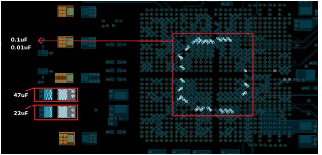
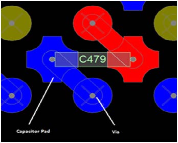
All decoupling capacitors (0.1 μF and 0.01 μF) must be 0402 or of a smaller package size, as they must be mounted on the back side of the board. They must fit between the adjacent vias of ball grid array (BGA) package pins. These decoupling capacitors are selected to have a low impedance over operating frequency and temperature range. Capacitor pad to via trace must be as small as possible. The following figure shows how these capacitors need to be mounted. Keep the capacitor pad directly on the corresponding vias. The capacitors must not share ground vias. Each decoupling capacitor must have its own via connection to the PCB ground plane.
- The Decoupling capacitor and the Smart Fusion2/IGOOL2 device can be placed side-by-side. If placed side-by-side, route the power with thick traces.Important: Microchip does not guarantee on noise on power rails. User must run the power simulation.
Figure 2-2. Capacitor Placement under BGA Vias