3.1 Timing Diagram Values
The following table lists the timing diagram values of the gate driver.
| Symbol | Parameter | Min. | Typ. | Max. | Unit | Notes |
|---|---|---|---|---|---|---|
|
TMIN |
Minimum pulse width |
1000 | — | — |
ns | — |
|
TD |
Delay time | — | — |
250 |
ns | — |
| — |
De-glitch time | — |
200 | — |
ns |
Input signal de-glitch time |
|
TR |
Rise time | — |
80 | — |
ns |
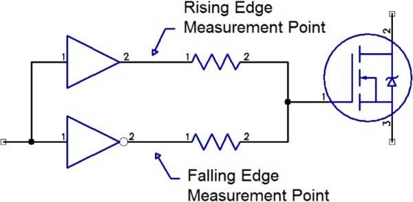
Measured from 10% to 90% points on edge measurement point 1 (see Figure 3-3) |
|
TF |
Fall time | — |
90 | — |
ns |
Measured from 10% to 90% points on edge measurement point 2 (see Figure 3-3) |
|
TS1 |
Two-level turn-off time | — |
360 | — |
ns |
Software configurable |
|
VSOFT |
Two-level turn-off voltage | — |
1.5 | — |
V |
Software configurable |
|
TDSAT |
Desaturation time |
1400 |
1500 |
1600 |
ns |
Software configurable |
|
VSOFTD1 |
First DSAT V | — |
9 | — |
V |
Multi-level turn-off—first DSAT step |
|
TSD1 |
First DSAT time3 | — |
400 | — |
ns |
First DSAT two-level turn-off time |
|
VSOFTD2 |
Second DSAT V | — |
5 | — |
V |
Multi-level turn-off—second DSAT step |
|
TSD2 |
Second DSAT time3 | — |
200 | — |
ns |
Second DSAT two-level turn-off time |
|
TFLT |
Fault time delay | — |
5000 | — |
ns | — |
|
Fault_Res |
Fault reset | — |
1000 | — |
ns | — |
|
TRESP |
Fault response time | — |
200 | — |
ns | — |
|
TNOV |
Dead time—input | — |
1000 | — |
ns |
Recommended minimum time between inputs |
|
TCOD |
Dead time—driver |
1000 | — | — |
ns |
Minimum time between drive signals allowed by driver, software configurable |
|
TRESET |
Reset timing |
1000 | — | — |
ns |
Minimum reset time |
| — |
Automatic reset (optional) | — |
5 | — |
ms |
Standard setting of 5 ms |
| — |
Main-secondary timing skew | — | — |
10 |
ns |
Timing difference between main and secondary drivers |
The following figure shows the measurement points for rise and fall time.