12.1.1 Chip Antenna and External Antenna (SMA Connector)
This section describes the PCB stack-up, mechanical details of the PCB trace leading up to SMA connector for case 1 and up to chip antenna for case 2. The host PCB can follow either of these trace designs to maintain compliance under the modular grant (FCC) and certificate (ISED). Schematics, BoM, Layout source files and Gerber files are available for download on the ATSAMR30M18A product web page.
- Trace width – 0.22 mm
- Trace gap – 0.42 mm
- Finished copper weight – 1 ounce
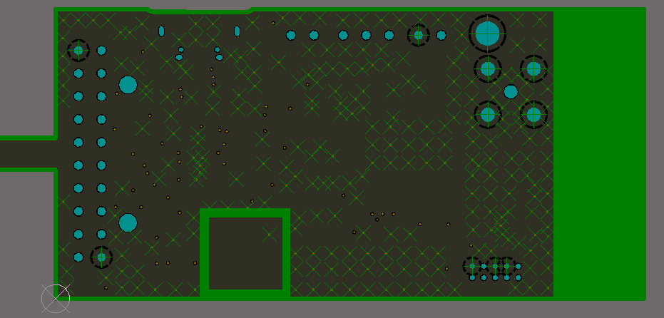
The following figure shows the top layer routing of the complete reference board (SAMR30 Module XPRO). The complete design documentation of the reference board is available on the SAMR30 Module XPRO Product web page.
- For a design with an external antenna through the RF connector(1), the RF trace running from L106 to chip antenna can be replaced with GND polygon pour (with distributed GND Vias). The PCB area containing the chip antenna footprint and the RF trace can be cut out.
- For a design using a chip antenna, the RF trace running from R115 to the RF connector(1), the RF connector(1) footprint can be replaced with a GND polygon pour (with distributed GND Vias).
- If the host board of ATSAMR30M18A is designed to have an antenna port that is accessible to the end-user, an RP (Reverse Polarity)-SMA socket must be used. If an RF coaxial cable is used between the module RF output and the enclosure, an RP-SMA connector must be used in the enclosure wall for interface with the antenna.
The following figure shows the top layer layout of the reference board focused on the RF traces. The snapshot also indicates the critical dimensions that are required to be replicated in the design to maintain compliance.

The technical specification of the approved chip and external antenna is listed in Table 11-1.
