
1.4.2 CPHA = 1 and CPOL = 0 (Mode 2) And CPHA = 1 And CPOL = 1 (Mode 3)
Like in the previous cases the falling edge of the SS lines selects and activates the slave. Compared to the previous cases, where CPHA equals zero, the transmission is not started and the MSB is not output by the slave at this stage.
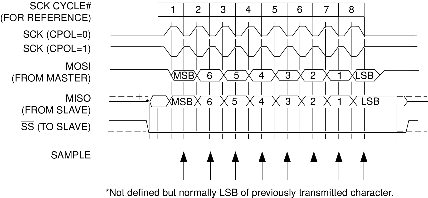
The actual transfer is started by a software write to the SPDR of the master what causes the clock signal to be generated. The first edge of the SCK signal from its inactive to its active state (rising edge if CPOL equals zero and falling edge if CPOL equals one) causes both the master and the slave to output the MSB of the byte in the SPDR. As shown in the preceding figure there is no delay of half a SCK-cycle like in Mode 0 and 1. The SCK line changes its level immediately at the beginning of the first SCK-cycle. The data on the input lines is read with the edge of the SCK line from its active to its inactive state (falling edge if CPOL equals zero and rising edge if CPOL equals one).
After eight clock pulses the transmission is completed, in both the master and the slave device the SPI interrupt flag (SPIF) is set and the received byte is transferred to the receive buffer.