
1.4.1 CPHA = 0 and CPOL = 0 (Mode 0) And CPHA = 0 And CPOL = 1 (Mode 1)
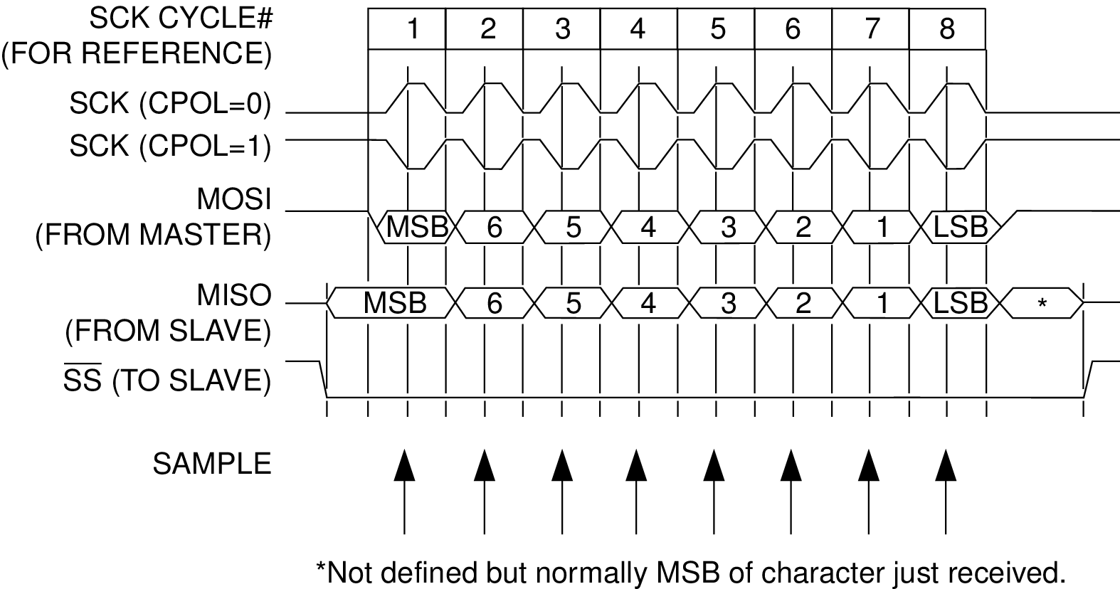
When the SPI is configured as a slave, the transmission starts with the falling edge of the SS line. This activates the SPI of the slave and the MSB of the byte stored in its data register (SPDR) is output on the MISO line. The actual transfer is started by a software write to the SPDR of the master. This causes the clock signal to be generated. In cases where the CPHA equals zero, the SCK signal remains zero for the first half of the first SCK cycle. This ensures that the data is stable on the input lines of both the master and the slave. The data on the input lines is read with the edge of the SCK line from its inactive to its active state (rising edge if CPOL equals zero and falling edge if CPOL equals one). The edge of the SCK line from its active to its inactive state (falling edge if CPOL equals zero and rising edge if CPOL equals one) causes the data to be shifted one bit further so that the next bit is output on the MOSI and MISO lines.
After eight clock pulses the transmission is completed. In both the master and the slave device the SPI interrupt flag (SPIF) is set and the received byte is transferred to the receive buffer.