
5.5 Gate Resistor Selection
The most crucial time interval of the gate drive is the turn ON and turn OFF of the MOSFET, and the key is performing this function quickly but with minimal noise and ringing to the overall system. Too fast a rise/fall time can cause unnecessary ringing and poor EMI, and too slow a rise/fall time will increase switching losses in the MOSFET.
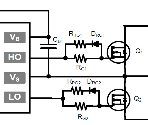
Considering the gate driver components for MCP14H2304 in Figure 5-6, with the careful selection of RG1 and RRG1, it is possible to selectively control the rise time and fall time of the gate drive to the MOSFET. For turn ON, all current will go from the IC through RG1 and charge the MOSFET gate capacitance, hence increasing or decreasing RG1 will increase or decrease rise time in the application. With the addition of DRG1 , the fall time can be separately controlled as the turn off current flows from the MOSFET gate capacitance, through RRG1 and DRG1 to the driver in the IC to VS for high side and COM for low side. So increasing or decreasing RRG1 will increase or decrease the fall time. Sometimes finer control is not needed and only RG1 and RG2 is used.
Increasing turn ON and turn OFF has the effect of limiting ringing and noise due to parasitic inductances, hence with a noisy environment, it may be necessary to increase the gate resistors. Gate component selection is a compromise of faster rise time with more ringing, and a poorer EMI but better efficiency, and a slower rise time with better EMI, better noise performance but poorer efficiency. The exact value depends on the parameters of the application and system requirements. Generally, for motors, the switching speed is slower, the deadtime is longer, and the application has more inherent noise, hence higher values are recommended, for example RGx = 10Ω - 100Ω. For power supplies, the switching speed is faster, deadtimes are shorter for efficiency, and so smaller values are typically used, for example RGx = 3Ω ~ 20Ω.
To have equal switching times for high-side and low-side, it is recommended that the gate driver components for high-side and low-side are mirrored. For example RRG1 = RRG2, DRG1 = DGR2, and RG1 = RG2.