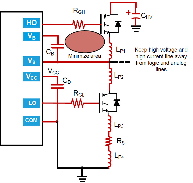
5.11 PCB Layout Suggestions
Layout plays a considerable role since unwanted noise coupling, unpredicted glitches and abnormal operation could arise due to poor layout of the associated components. Figure 5-10 shows the schematic with parasitic inductances in the high current path (LP1, LP2, LP3, LP4) which would be caused by inductance in the metal of the trace. Considering Figure 5-10, the length of the tracks in red should be minimized, and the bootstrap capacitor (CB) and the decoupling capacitor (CD) should be placed as close to the IC as possible, in addition to using low ESR ceramic capacitors. Finally, the gate resistors (RGH and RGL) and the sense resistor (RS) should be surface mount devices. These suggestions will reduce the parasitics caused by the PCB traces.