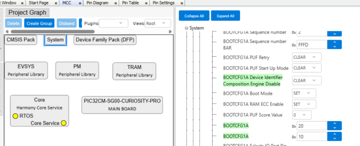
14.1 MCC Configuration
MPLAB Code Configurator (MCC v4) configuration for the PIC32CMSG00 LED demo application. The
configuration file is located at
pic32cmsg_led_app.X/pic32cmsg_led_app_default/mcc-config.mc4.
Target Device
| Parameter | Value |
|---|---|
| Device | PIC32CM5112SG00100 |
| Architecture | Arm Cortex-M23 (Armv8-M with TrustZone) |
| Board | PIC32CM-SG00-CURIOSITY-PRO |
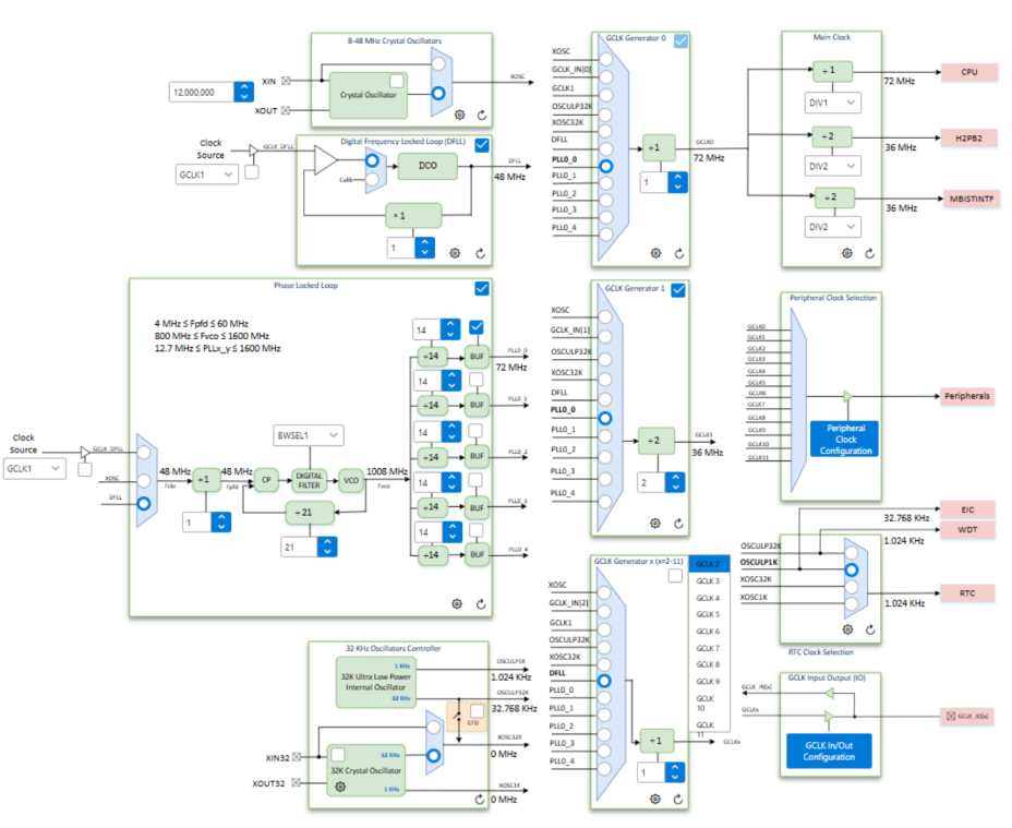
Clock Configuration
| Parameter | Value |
|---|---|
| CPU Clock (MCLK Domain 0) | 72 MHz |
| MCLK Domain 1 | 36 MHz (CPU/2) |
| MCLK Domain 2 | 36 MHz (CPU/2) |
| PLL0 Reference Source (REFSEL) | 2 (internal oscillator) |
| PLL0 Feedback Divider (FBDIV) | 21 |
| PLL0 Post Divider 0 (POSTDIV0) | 14 |
| GCLK0 Source | PLL0 output 0, divider 1 (72 MHz) |
| GCLK1 Source | PLL0 output 0, divider 2 (36 MHz) |
| SERCOM4 Core Clock | GCLK1 = 36 MHz |
| SysTick Clock | Processor clock = 72 MHz |
| RTC Source (OSC32KCTRL) | ULPOSC32K |
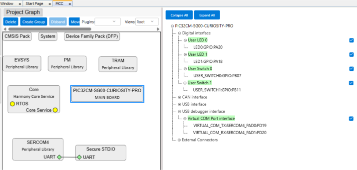
Peripheral Configuration (Secure Side)
| Peripheral | Configuration | Purpose |
|---|---|---|
| SERCOM4 (USART) | 115200-8-N-1, internal clock, 16x oversampling | Serial console (printf) |
| SYSTICK | 100 ms period (LOAD = 7,199,999), interrupt enabled | LED1 blink timer |
| PORT | PA18 output (Secure LED1), PD19/PD20 PMUX func D (SERCOM4) | GPIO + UART pins |
| EVSYS | Initialized (default) | Event system |
| PM | Default power manager | Power control |
| NVIC | Interrupts enabled | Interrupt controller |
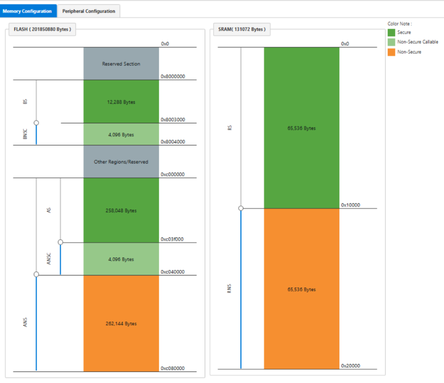
TrustZone / IDAU Configuration
| Region | Size | Notes |
|---|---|---|
| Non-Secure Flash (PFMANS) | 256 KB (0x40 pages x 4 KB) | Start:
0x0C040000 |
| NSC Region (PFMANSC) | 4 KB (1 page x 4 KB) | Veneer functions |
| Non-Secure RAM (DRM) | 16 KB (0x10 pages x 1 KB) | NS stack + data |
| Boot Flash NS (BFM) | 0 KB | No NS boot Flash |
| IDAU | Enabled + write-locked | - |
Pin Settings
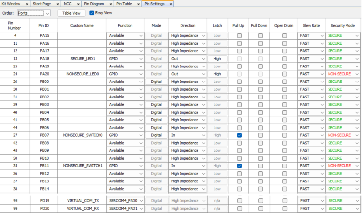
| Pin | Security | Function |
|---|---|---|
| PA18 | Secure | SECURE_LED1 (toggled by SysTick) |
| PA20 | Non-Secure | NONSECURE_LED0 (driven by NS app) |
| PB7 | Non-Secure | NONSECURE_SWITCH0 (input, pull-up) |
| PB11 | Non-Secure | NONSECURE_SWITCH1 (input, pull-up) |
| PD19 | Secure | SERCOM4 TX (virtual COM) |
| PD20 | Secure | SERCOM4 RX (virtual COM) |
Key Fuse for DICE Activation/Deactivation
If the BOOTCFG1 DICE Disable value is CLEAR, then Boot ROM will proceed with generating CDI. Otherwise, the Boot ROM will continue with boot process.
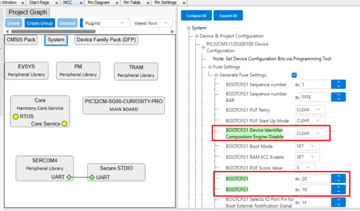
| Setting | Value | Description |
|---|---|---|
| BOOTCFG1 DICE Disable | CLEAR | DICE flow is enabled |
| BOOTCFG1 | 0x20 | DICE CDI Index. Generated CDI is stored in TRAM at WORD offset specified by this value. |
| BOOTCFG1 | 0x10 | DICE Firmware Hash Index. Implementation gets the FW HASH starting from the TRAM WORD offset specified by this value to calculate CDI. |
Both BOOTCFG1 and BOOTCFG1A must be programmed with same valid fuses.