43.1.13 External XTAL and Clock AC Electrical Specifications
Table 43-17. External XTAL and Clock AC Electrical Specifications
AC Characteristics
Standard Operating Conditions: VDD = 1.9V to 3.6V (unless otherwise stated) Operating Temperature: -40°C ≤ TA ≤ +85°C for Industrial Temp -40°C ≤ TA ≤ +125°C for Extended Temp
Param. No.
Symbol
Characteristics
Min.
Typ.
Max.
Units
Conditions(1)
XOSC_1
FOSC_XOSC
External CLKI frequency
—
16
—
MHz
XIN, XOUT Primary Osc
EC (±20 ppm)
XOSC_1A
TOSC
TOSC = 1/FOSC_XOSC
—
0.0625
—
ns
See parameter XOSC_1 for FOSC_XOSC value
XOSC_2
XOSC_ST(3)
XOSC crystal start-up time
—
—
2.5
ms
Crystal stabilization time only not oscillator ready
XOSC_3
CXIN
XOSC XIN parasitic pin capacitance
—
0.35
—
pF
With default crystal trim settings
XOSC_5
CXOUT
XOSC XOUT parasitic pin capacitance
—
0.35
—
pF
With default crystal trim settings
XOSC_11
CLOAD(4)
XOSC crystal FOSC = 16 MHz
—
9
—
pF
—
XOSC_21
ESR
XOSC crystal FOSC = 16 MHz
—
—
100
Ω
—
XOSC_33
DLEVEL
MCU crystal oscillator power drive level
—
100
—
μW
—
XOSC_34
Gm
XOSC Transconductance
14
16
18
mA/V
XOSC Auto gain control disabled
VDD = 1.2V, TA = +25°C
Note:
VDDIO = AVDD = 3.3V.
The parameters are characterized but not tested in manufacturing.
This is for guidance only. A major component of crystal start-up time is based on the 2nd party crystal MFG parasitics that are outside the scope of this specification. If this is a major concern, the customer must characterize this based on their design choices.
The test conditions for the crystal load capacitor calculation are as follows:
Standard PCB trace capacitance = 1.5 pF per 12.5 mm (0.5 inches) (in other words, PCB STD TRACE W = 0.175 mm, H = 36 μm, T = 113 μm).
Xtal PCB capacitance typical; therefore, ~= 2.5 pF for a tight PCB xtal layout
For CXIN and CXOUT within 4 pF of each other, assume CXTAL_EFF = ((CXIN+CXOUT)/2).
Note: Averaging CXIN and CXOUT will affect the final calculated CLOAD value by less than 0.25 pF.
Equation 43-1. Equation 1:
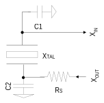
Assuming C1 = C2 and CXin ~= CXout, the formula can be further simplified and restated to solve for C1 and C2 by:
Equation 43-2. Equation 2 (In other words: Simplified Equation 1)
C1 = C2 = 13 pF (in other words, for hypothetical example crystal external load capacitors)
User C1 = C2 = 13 pF CLOAD (max) spec
The maximum start-up time is user-selectable in XOSCCTRL.STARTUP.
Figure 43-1. External XTAL and Clock Diagram
The online versions of the documents are provided as a courtesy. Verify all content and data in the device’s PDF documentation found on the device product page.