
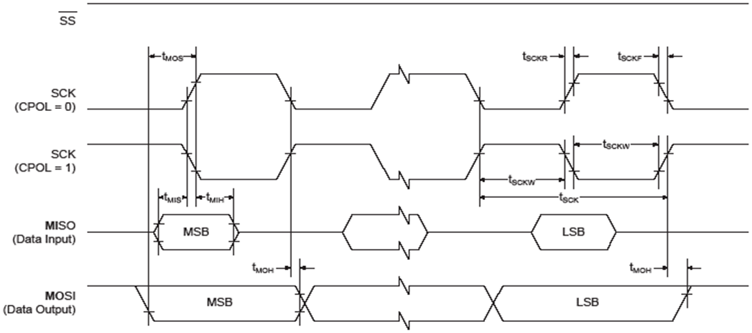
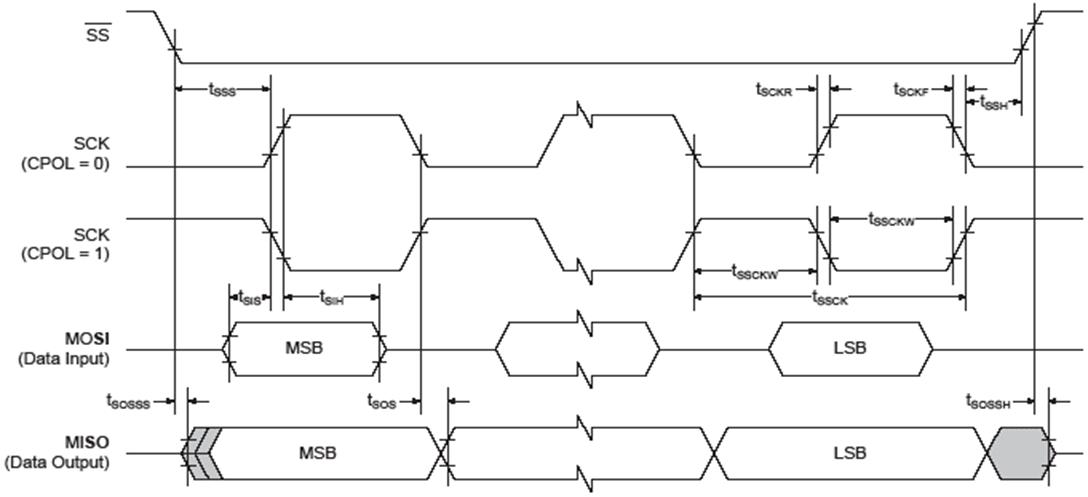
15.13.2 SERCOM in SPI Mode in PL0
| Symbol | Parameter | Conditions | Min. | Typ. | Max. | Units | |
|---|---|---|---|---|---|---|---|
| tSCK | SCK period | Master, VDD>2.70V | 141 | 153 | ns | ||
| Master, VDD>1.8V | 147 | 159 | |||||
| tSCKW | SCK high/low width | Master | - | 0.5*tSCK | - | ||
| tSCKR | SCK rise time(2) | Master | - | 0.25*tSCK | - | ||
| tSCKF | SCK fall time(2) | Master | - | 0.25*tSCK | - | ||
| tMIS | MISO setup to SCK | Master, VDD>2.70V | 141 | ||||
| Master, VDD>1.8V | 147 | ||||||
| tMIH | MISO hold after SCK | Master, VDD>2.70V | 0 | ||||
| Master, VDD>1.8V | 0 | ||||||
| tMOS | MOSI setup SCK | Master, VDD>2.70V | 30 | ||||
| Master, VDD>1.8V | 30.6 | ||||||
| tMOH | MOSI hold after SCK | Master, VDD>2.70V | -9 | ||||
| Master, VDD>1.8V | -8.5 | ||||||
| tSSCK | Slave SCK Period | Slave, VDD>2.70V | 220 | 250 | |||
| Slave, VDD>1.8V | 230 | 250 | - | ||||
| tSSCKW | SCK high/low width | Slave | - | 0.5*tSCK | - | ||
| tSSCKR | SCK rise time(2) | Slave | - | 0.25*tSCK | - | ||
| tSSCKF | SCK fall time(2) | Slave | - | 0.25*tSCK | - | ||
| tSIS | MOSI setup to SCK | Slave, VDD>2.70V | 42 | - | - | ||
| Slave, VDD>1.8V | 42 | ||||||
| tSIH | MOSI hold after SCK | Slave, VDD>2.70V | 0 | ||||
| Slave, VDD>1.8V | 0 | ||||||
| tSSS | SS setup to SCK | Slave | PRELOADEN=1 | ||||
| PRELOADEN=0 | |||||||
| tSSH | SS hold after SCK | Slave | |||||
| tSOS | MISO setup before SCK | Slave, VDD>2.70V | 109 | ||||
| Slave, VDD>1.8V | 115 | ||||||
| tSOH | MISO hold after SCK | Slave, VDD>2.70V | 17.3 | ||||
| Slave, VDD>1.8V | 17.3 | ||||||
| tSOSS | MISO setup after SS low | Slave, VDD>2.70V | 95 | ||||
| Slave, VDD>1.8V | 102 | ||||||
| tSOSH | MISO hold after SS high | Slave, VDD>2.70V | 10.2 | ns | |||
| Slave, VDD>1.8V | 10.2 | ||||||
Note: 1. These values are based on simulation. They are not covered
by production test limits or characterization.
Maximum SPI Frequency
- Master Mode
fSCKmax = 1/2*(tMIS + tvalid), where tvalid is the slave time response to output data after detecting an SCK edge. For a non-volatile memory with tvalid = 12ns Max, fSPCKMax = 3.7MHz @ VDDIO > 2.7V
- Slave Mode
fSCKmax = 1/2*(tSOV + tsu), where tsu is the setup time from the master before sampling data. With a perfect master (tsu=0), fSPCKMax = 6MHz @ VDDIO > 2.7V