
2.1.1 Transceiver Reference Clock Configurator
(Ask a Question)The Transceiver Reference Clock Configurator is used to build the correct reference clock input to the transceiver and to the Tx PLL. The user can pick the input type and various input options.
To initiate the Reference Clock Configurator, perform the following steps:
- Access the Transceiver Reference Clock cores under Features from the Catalog window, as shown in the following figure.
Figure 2-1. Transceiver Reference Clock Selection from Catalog 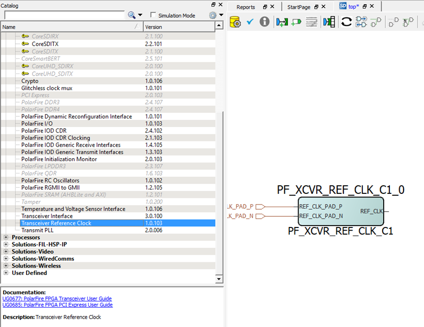
- Double-click each PF_XCVR_REF_CLK block from the
catalog to launch the configurator. A GUI allows the selection of the related
reference clock properties.
Figure 2-2. Transceiver Reference Clock Configurator GUI 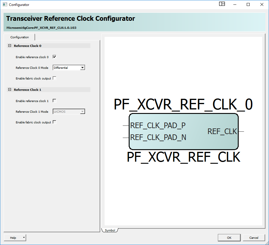
The following table lists transceiver reference clock configurator GUI options.
Table 2-2. Transceiver Reference Clock Configurator GUI Options Options Default Details Reference Clock 0 Configuration Enable reference clock 0 Enable and disable Enabled Checked = enabled Reference Clock 0 Mode LVCMOS, voltage reference, and differential Differential Enable fabric clock output Enable and disable Disabled Checked = enabled When enabled, a port is exposed for fabric routing.
Reference Clock 1 Configuration Enable reference clock 1 Enable and disable Disabled Checked = enabled Reference Clock 1 Mode LVCMOS and voltage reference LVCMOS Enable fabric clock output Enable and disable Disabled Checked = enabled When enabled, a port is exposed for fabric routing.
- Select the reference clock mode type based on the
input buffer type in the application.
Single-ended Differential is the
default mode.
Figure 2-3. Transceiver Reference Clock Mode Type 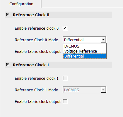
In the case of LVCMOS or Voltage Reference inputs, the design can have up to two individual reference clock inputs in one instance of the PF_XCVR_REF_CLK. This configuration can access either or both Reference Clock 0 or/and 1.
Figure 2-4. PF_XCVR_REF_CLK With One Single-Ended Input and Single Output Clock 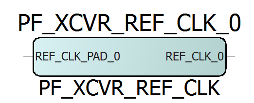
Figure 2-5. PF_XCVR_REF_CLK With Two Single-Ended Input and Two Output Clock 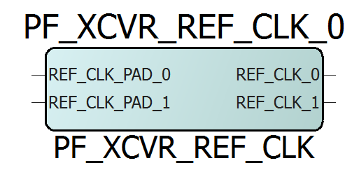
However, only one reference clock input is available when the designer selects Differential (Figure 3). In this case, only Reference Clock 0 can be accessed and use a differential clock source signal.
Figure 2-6. PF_XCVR_REF_CLK With Differential Input and Single Output Clock 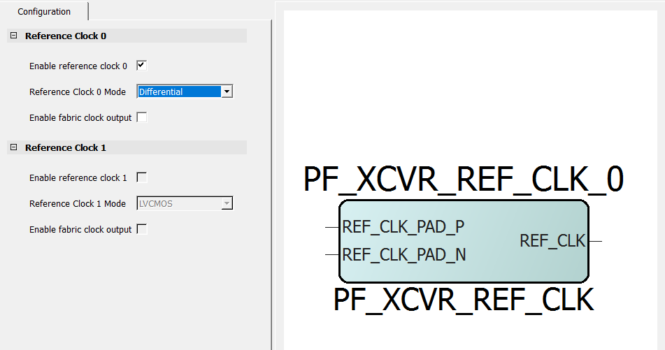
- Optionally enable a connection to the FPGA fabric for either/both reference clock 0 or reference clock 1. When enabled, a related port of the associated reference clock is exposed for fabric routing.
Figure 2-7. PF_XCVR_REF_CLK With Fabric Output Clock 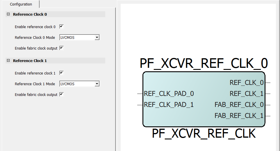
- Click OK after making desired selections.
When the Reference Clock configurator generates the reference clock block, specify the desired IP Standard. This is completed by adding the desired IO to the PDC file. For more information about adding the IO to the PDC file, see Physical Constraints.
For more information about XCVR REFCLK input configuration, see XCVR REFCLK Usage.
The PF_XCVR_REF_CLK allows a global routing connection to the FAB_REF_CLK output through a CLKINT global buffer. The FAB_REF_CLK output uses regular fabric routing resources and the connection traverse half the device before connecting onto a CLKINT fabric Global Buffer at the center of the chip. FAB_REF_CLK clock is potentially more susceptible to fabric switching noise, depending on the design, which could lead to an unpredictable amount of clock jitter on that clock being broadcasted to the fabric.