2.1.2 Transmit PLL Configurator
(Ask a Question)The Transceiver Transmit PLL Configurator is used to build the correct transmit PLL to the transceiver. The user can pick from many of the PLL options used for the transceiver based on the application.
To initiate the Transceiver Transmit PLL Configurator, perform the following steps:
- Access the Transmit PLL module under Features from the Catalog window, as shown in the following figure.
Figure 2-8. Transceiver Transmit PLL Selection from Catalog 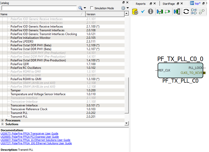
- Double-click each PF_TX_PLL block from the catalog to launch the configurator. A GUI allows the option of selecting the related transmit PLL properties.
Figure 2-9. Transmit PLL Configurator GUI 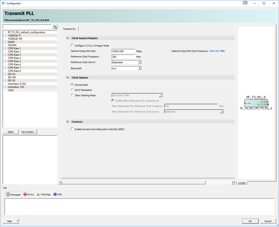
The following table lists the transmit PLL configurator GUI options.
Table 2-3. Transmit PLL Configurator GUI Options Clock Inputs Options Default Details Configure Tx PLL in Integer Mode Enable and disable Disabled When disabled, it is in TXPLL Fractional N Mode. When enabled, it allows fixed value of available reference clock frequencies. Reference Clock Source Dedicated and fabric Dedicated Dialogue box requires input clock rate (200 MHz default) Desired Output Bit Clock VCO rate, and output clock (MHz) 10000 Mbps, 5000 MHz Only valid combinations can be entered based on reference clock and PLL capability. This value represents the BIT_CLK output speed. Bandwidth Low/High Low By default, the Tx PLL selects the low bandwidth option in order to filter more of the reference clock jitter. If the system has a low-jitter reference clock, the user can then set it to high bandwidth mode to decrease the overall jitter. Low bandwidth has longer lock times than high bandwidth. Clock options (Only one option can be selected) Normal Mode Enable and disable Enabled Radio-button on = enabled SSCG Modulation Enable and disable Enabled Radio-button on = disabled Jitter Cleaning Mode Enable and disable Disabled Radio-button on = disabled The following options are available when enabled: 10G SyncE 32Bit
10G SyncE 64Bit
1G SyncE 10Bit
CPRI Rate 1
CPRI Rate 2
CPRI Rate 3
CPRI Rate 4
CPRI Rate 5
CPRI Rate 6
CPRI Rate 8 – 64-bit
SDI 3G
SDI HD
SDI SD
Custom Protocol Settings
Features Enable Dynamic Reconfiguration Interface (DRI) Enable and disable Disabled Adds Pins to TXPLL component for using Dynamic Reconfiguration Interface. See PolarFire Family Device Power-Up and Resets User Guide for DRI information. Note: For information about pin functions, see Table 1-18. - Select one of the Reference Clock sources (dedicated source is the default) to define Clock Inputs and enter the reference clock value.
Figure 2-10. Clock Inputs 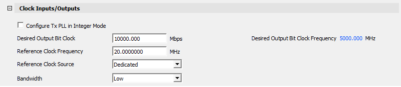
- Enter the values in Desired Output Bit Clock. Frequency cannot be entered—it is calculated automatically based on the speed (data rate in Mbps) and the reference clock.
Figure 2-11. Fabric Clock Input 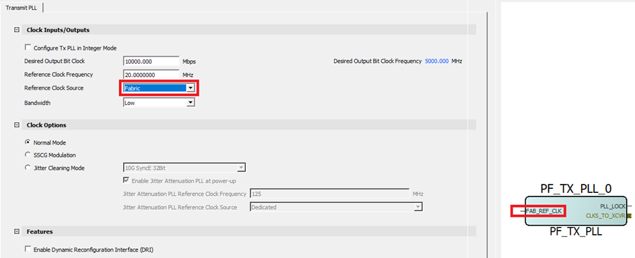
Normal Mode configures the TX PLL to default operation based on the clock Inputs/Outputs setting. Whereas, Jitter Cleaning mode customizes the attenuation coefficients for the pre-defined standards to be used where the recovered clock can be used as a TX reference clock to meet protocol jitter specifications.
Figure 2-12. Clock Options 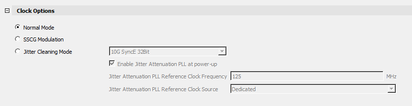
- Click Spread Spectrum clock generation mode (Not available prior to Libero SoC v12.3). This feature allows spread-spectrum generation to be enable from the transmit phase-locked loop. See respective
PolarFire FPGA Datasheet
, RT PolarFire FPGA Datasheet or
PolarFire SoC Datasheet
for more information on spread spectrum specifications.
Figure 2-13. Spread Spectrum Clock Generation Enable 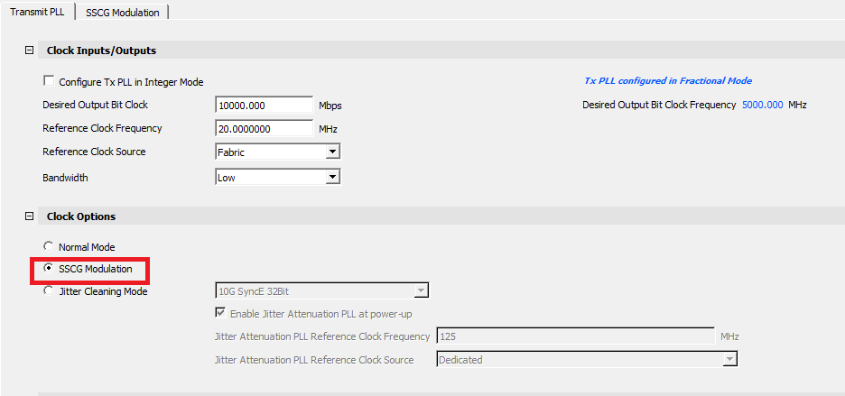
- Select SSCG mode to enable the SSCG Modulation Feature tab.
Figure 2-14. Spread Spectrum Modulation Options 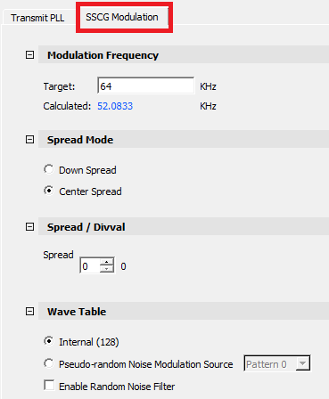
- Click OK after making desired selections.
For more information about Spread Spectrum, see Spread Spectrum Clocking.
Table 2-4. Spread Spectrum Options Default Details Modulation Frequency Target User entry 64 KHz Target Spread Spectrum modulation. Calculated 60.0962 KHz Calculation is based on TXPLL reference clock settings. Spread Mode Down spread/Center Spread Down Configures the modulation style Spread/Divval Spread Pull down 0 Sets up to 32 divider settings (0, 01.,....3.1). This value sets the percent of modulation amplitude down or center spread. Wave Table Internal (128) Enabled Selects internal 128 point triangle wave Pseudo-random Noise Modulation Source Disabled Selection between 3 predefined modulation patterns. Enable Random Noise Filter Enable/Disable1 Disabled Enable to turn on filtering to reduce jitter if needed. (1) When pseudo-random noise modulation source is enabled after the user selects one of the predefined modulation patterns. The optional high pass filtered PRBS is modulated to the PLL reducing the harmonic frequency amplitude peaks. For more information about jitter cleaning operation, see Jitter Attenuator.
- Click Enable Dynamic Reconfiguration Interface (DRI) checkbox to add the ports needed to connect the Transmit PLL to the DRI. See PolarFire Family Device Power-Up and Resets User Guide for more information about DRI usage and specifications.
Figure 2-15. Enable Dynamic Reconfiguration Interface 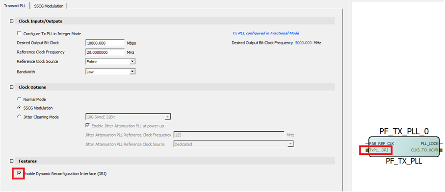
- Click OK after making desired selections.
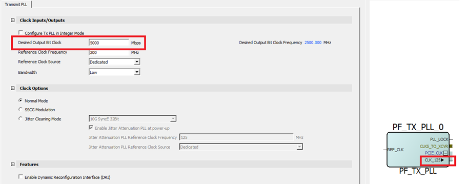
The TxPLL supports an additional clock output. This CLK_125 output port is automatically exposed when TxPLL BIT_CLK is 5 Gbps. This clock is used with the PCIE macro as input to the transaction layer or AXI clock. For more information about CLK_125, see PolarFire Family PCI Express User Guide.