
2.1.3 Transceiver Interface Configurator
(Ask a Question)The Transceiver Interface Configurator is used to build the transceiver based on protocol requirements. The user selects the number of lanes, data rate, and protocol-specific settings.
To initiate the Transceiver Interface Configurator, perform the following steps:
- Access the Transceiver Interface module
under Features from the Catalog window, as shown in the following figure.
Figure 2-17. Transceiver Interface Selection From Catalog 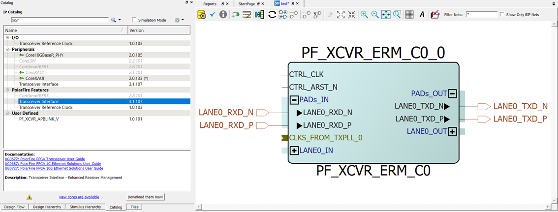
- Double-click each PF_XCVR block in the catalog to
launch the configurator. A GUI allows the option to select the related XCVR properties.
Figure 2-18. Transceiver Interface Configuration GUI 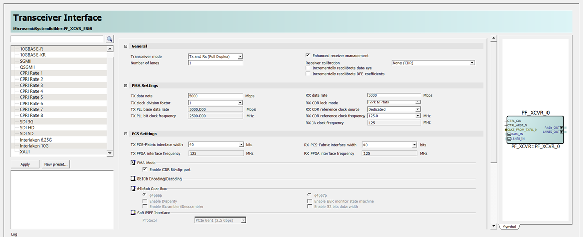
The following tables list Transceiver Interface options.
Table 2-5. Transceiver Interface General Settings General Options Default Details Number of lanes 1 to 4 1 Transceiver mode Tx and Rx (Full Duplex) Tx and Rx (Full Duplex) See Transceiver Modes for more information. Tx Only Rx Only Tx and Rx (Independent) Enhanced Receiver Management Enable/Disabled Enabled Includes the enhanced receiver management solution when checkbox is checked (See Enhanced Receiver Management). Receiver Calibration None (CDR), On-Demand, On-Demand & First Lock, and None (DFE), Incrementally Recalibrate Data Eye and Incrementally Recalibrate DFE Coefficients
On-Demand & First Lock See Receiver. Table 2-6. Transceiver Interface PMA Settings PMA Settings Options Default Details Tx data rate 250 – 12700 Mbps 5000 Mbps 10312.5 Mbps (STD maximum) TX clock division factor 1, 2, 4, 8, and 11 1 — TXPLL base data rate Computed1 — — TX PLL bit clock frequency Computed — — RX Data rate 250 Mbps – 12700 Mbps 5000 Mbps 10312.5 Mbps (STD maximum) RX CDR lock mode Lock to reference, Lock to data, Burst Mode Receiver2, lock to data with 2x gain3 Lock to data — RX CDR reference clock source Dedicated and fabric Dedicated — RX CDR reference clock frequency4 Based on transceiver data rate — — RX JA Clock Frequency Calculated based on configuration — — Note:- Enter the transceiver data rate (lane rate), and the TX clock division factor in the XCVR UI. Based on these settings, the TX_PLL base data rate is calculated. The TX_BIT_CLK frequency is half of the TX_PLL base data rate. The TX_PLL base data rate must be entered under the desired output clock option of the PF_TX_PLL block. The PF_TX_PLL generates the BIT_CLK output (connected to the TX_BIT_CLK_0/1 input of PF_XCVR).
- When Burst Mode Receiver (BMR) is selected, LANE_X_CDR_LOCKMODE[1:0] port is exposed.
- Default Gain, slower CDR lock time, lower jitter tolerance 2x Gain, faster CDR lock time, higher jitter.
- This input frequency is given by the user to support the integer feedback divider of the receiver PLL. From the drop-down, enter a CDR reference clock frequency (MHz) value equal to the reference clock used to the Receiver PLL. The computation derives the feedback divider used to clock the receiver data path.
Table 2-7. Transceiver Interface PCS Settings PCS Settings Options Default Details PCS-fabric interface width 8, 10, 16, 20, 32, 40, 64, and 801 40 — FPGA interface frequency2 Computed — — PMA Mode Enable CDR Bit-slip port Enable — 8b10b encoding/decoding None — — 64b6xb gear box 64b66b 64b67b
64b66b If 64b6xb mode is enabled, then PCS-Fabric interface width must be 32- or 64-bit. 64b66b gear box3 Enable disparity Disabled Enabled for 64b67b Enable scrambler/de-scrambler Disabled — Enable BER monitor state machine Disabled — Enable 32 bits data width Disabled — 64b67b gear box3 Enable BER monitor state machine Disabled Enable 32 bits data width Enable Disparity Disabled Cannot be enabled for 64b66b Enable Scrambler/de-scrambler Disabled — Enable 32 bits data width Disabled — Soft PIPE interface PCIe Gen1 (2.5 Gbps) PCIe Gen2 (5.0 Gbps) PCIe Gen1 (2.5 Gbps) — Note:- Dependent on PCS settings.
- TX_CLK_G/R frequency = RX_CLK_G/R frequency = FPGA Interface frequency = data rate/(PMA-PCS width × PCS Gearing).
- When 64b6xb Gear Box is enabled, the Enable Disparity, Enable BER monitor state machine, Enable Scrambler/Descrambler, and Enable 32 bits data width options can be enabled or disabled independently for both 64b66b and 64b67b.
Table 2-8. Clocks and Resets Interface Options Options Default Details Interface clock Use as PLL reference clock Disabled When Use as PLL reference clock is selected, this exposes additional ports that permit connection to the PLL REFCLKs. LANEn_TX_CLK_TO_PLL_REFCLK
LANEn_RX_CLK_TO_PLL_REFCLK
This allow designs that require gearing other than 2:1 with wider fabric interfaces and use dedicated routing to the PLL. This is used in place of CLKDIV, which does not have the dedicated routing to PLL.
TX clock 2 Global, Regional, Regional (Deterministic), Global Shared Regional See Table 1-16 RX clock 2 Global, Regional, Regional (Deterministic), Global Shared, and NA Regional NA option must be selected when the PCS is configured in Soft PIPE mode (PCIe). See Table 1-16 Interface Resets PMA Reset1 TX and RX — PCS Reset1 Tx Only, Rx Only, Tx and Rx RX Only – only RX side can be reset from the fabric. TX Only – only TX side can be reset from the fabric.
TX and RX – both RX and TX sides can be reset from the fabric.
Optional Ports Enable/Disable — TX_BYPASS port/TX_ELEC_IDLE port. See Table 1-10 or Table 1-12.
RX_READY_CDR and RX_VAL_CDR ports. JA_CLK port. See Jitter Attenuator. Dynamic Reconfiguration Enable Dynamic Reconfiguration Interface (DRI) Disabled — Note:- The minimum pulse width required is 16 clock cycles.
- To toggle TX clock and RX clock, an active pulse is provided on PCS Reset and PMA Reset.
Preset configurations are available within the Transceiver Interface Configurator to speed up the transceiver configuration. Factory provided presets are available with the Libero release. Additionally, customized presets can be saved. See Transceiver Modes for more information.
- Select Number of lanes from 1 to 4 in the general settings configuration.
- Enter the Transceiver data rate and select one of the TX clock division factors. The TX PLL base data rate is calculated in the GUI. The calculated TX PLL base data rate must be entered under the desired output clock option inside the PF_TX_PLL configurator. LANE#_TX_PLL_REF_CLK_#, LANE#_TX_BIT_CLK_0, and LANE#_TX_PLL_LOCK_# are included in CLKS_FROM_TXPLL_# BIF (bus interface). This connection is required between the TXPLL and Transceiver Interface.
- Select the desired CDR reference clock
mode and CDR reference clock frequency from the drop-down list based on the
application.Important: CDR reference clock frequency drop-down list is populated with valid frequencies based on the data rate.
- Select the CDR reference clock source based on the design requirements. The dedicated clock adds a dedicated CDR_REF_CLK port whereas the fabric port only includes a port that can be connected to the fabric resources. The dedicated CDR_REF_CLK_0/1 port must be connected to the REF_CLK or REF_CLK_0/1 output of the PF_XCVR_REF_CLK block.
- Select PCS-Fabric interface width from the GUI. This selection computes the FPGA interface frequency. The FPGA interface frequency is calculated based on the transceiver data rate, PCS-Fabric width, and the PCS settings/mode.
- Click the GUI radio button to select the desired PCS mode. See Transceiver PCS Interface Modes for more information on PCS mode.
- Select the desired interface clock options in the Interface Options GUI. See PCS/FPGA Fabric Interface.
- For PMA Only modes - CDR Bit-slip, select the
Enable CDR Bit-slip port to add the LANE#_RX_SLIP pin.
Figure 2-19. PMA Mode—Enable CDR Bit-Slip Port 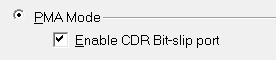
Figure 2-20. XCVR Component With CDR Bit-Slip Port Enabled 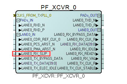 Important: For information about RX_SLIP, see Bit Slip.
Figure 2-21. XCVR Component With BMR Port Enabled 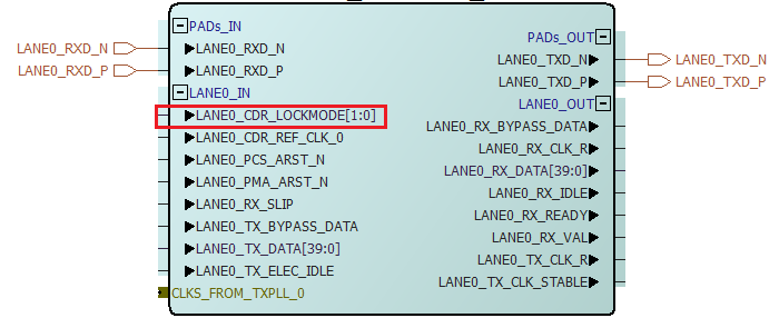 Important: For information about CDR_LOCKMODE pins, see burst mode receiver in CDR Options.
 - Select the Enable Dynamic Reconfiguration
to add the LANE#_DRI_SLAVE pins. See Dynamic Reconfiguration Interface for usage details.
Figure 2-22. XCVR Component With DRI Port Enabled 
- After making all of the selections in the Transceiver Interface Configurator, click OK.
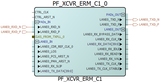
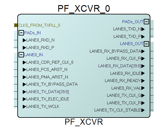
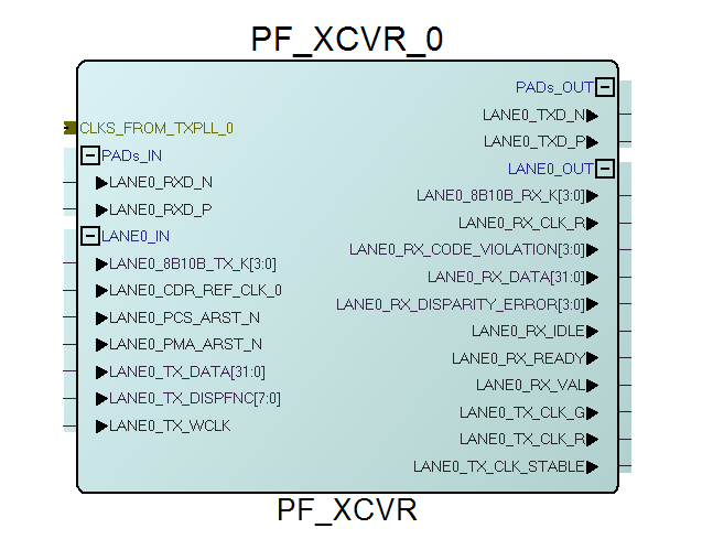
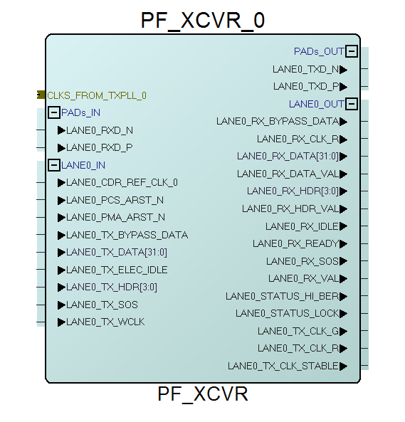
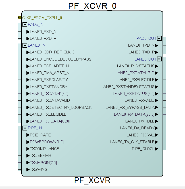
When the transceiver interface configuration is complete, a PF_XCVR macro is generated by the Libero Software. The macro includes the ports based on the configuration. Figure 7 to Figure 11 shows sample PCS macros. The PF_XCVR macro is instantiated into the user design to customize the connectivity of the application.
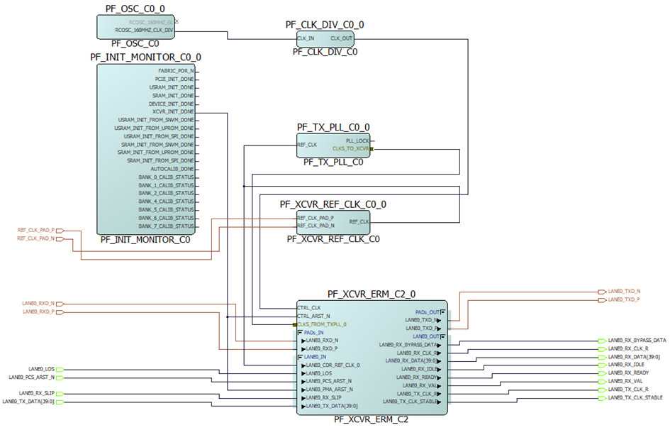
After building the PF_XCVR, PF_TX_PLL, and PF_XCVR_REF_CLK cores, the transceiver subsystem must be connected together in the SmartDesign canvas. Typically, the REF_CLK and/or FAB_REF_CLK outputs of the PF_XCVR_REF_CLK are connected to the respective inputs of the PF_XCVR and the input REF_CLK of the PF_TX_PLL. LANE#_TX_PLL_REF_CLK_#, LANE#_TX_BIT_CLK_0, and LANE#_TX_PLL_LOCK_# are included in CLKS_FROM_TXPLL_# BIF (bus interface). This connection is required between the TXPLL and transceiver interface. The SmartDesign component must then be generated.

See the port list tables in Transceiver PCS Interface Modes for complete pin descriptions generated with the Transceiver Configurator.