
16.3.5 MACC
(Ask a Question)16.3.5.1 MACC
(Ask a Question)18-bit x 18-bit multiply-accumulate MACC block. The MACC block can accumulate the current multiplication product with a previous result, a constant, a dynamic value, or a result from another MACC block. Each MACC block can also be configured to perform a Dot-product operation. All the signals of the MACC block (except CDIN and CDOUT) have optional registers.

| Port Name | Direction | Type | Polarity | Description |
|---|---|---|---|---|
| DOTP | Input | Static | High | Dot-product mode.
|
| SIMD | Input | Static | — | Reserved. Must be 0. |
| OVFL_CARRYOUT_SEL | Input | Static | High | Generate OVERFLOW or CARRYOUT with result P. OVERFLOW when OVFL_CARRYOUT_SEL = 0 CARRYOUT when OVFL_CARRYOUT_SEL = 1 |
| CLK[1:0] | Input | Dynamic | Rising edge | Input clocks. CLK[1] is the clock for A[17:9], B[17:9], C[43:18], P[43:18], OVFL_CARRYOUT, ARSHFT17, CDSEL, FDBKSEL and SUB registers. CLK[0] is the clock for A[8:0], B[8:0], C[17:0], CARRYIN and P[17:0]. In normal mode, ensure CLK[1] = CLK[0]. |
| A[17:0] | Input | Dynamic | High | Input data A. |
| A_BYPASS[1:0] | Input | Static | High | Bypass data A registers. A_BYPASS[1] is for A[17:9]. Connect to 1, if not registered. A_BYPASS[0] is for A[8:0]. Connect to 1, if not registered. In normal mode, ensure A_BYPASS[0] = A_BYPASS[1]. |
| A_ARST_N[1:0] | Input | Dynamic | Low | Asynchronous reset for data A registers. Connect both A_ARST_N[1] and = A_ARST_N[0] to 1 or to the global Asynchronous reset of the design |
| A_SRST_N[1:0] | Input | Dynamic | Low | Synchronous reset for data A registers. A_SRST_N[1] is for A[17:9]. Connect to 1, if not registered. A_SRST_N[0] is for A[8:0]. Connect to 1, if not registered. In normal mode, ensure A_SRST_N[1] = A_SRST_N[0]. |
| A_EN[1:0] | Input | Dynamic | High | Enable for data A registers. A_EN[1] is for A[17:9]. Connect to 1, if not registered. A_EN[0] is for A[8:0]. Connect to 1, if not registered. In normal mode, ensure A_EN[1] = A_EN[0]. |
| B[17:0] | Input | Dynamic | High | Input data B. |
| B_BYPASS[1:0] | Input | Static | High | Bypass data B registers. B_BYPASS[1] is for B[17:9]. Connect to 1, if not registered. B_BYPASS[0] is for B[8:0]. Connect to 1, if not registered. In normal mode, ensure B_BYPASS[0] = B_BYPASS[1]. |
| B_ARST_N[1:0] | Input | Dynamic | Low | Asynchronous reset for data B registers. In normal mode, ensure Connect both B_ARST_N[1] and B_ARST_N[0] to 1 or to the global Asynchronous reset of the design. |
| B_SRST_N[1:0] | Input | Dynamic | Low | Synchronous reset for data B registers. B_SRST_N[1] is for B[17:9]. Connect to 1, if not registered. B_SRST_N[0] is for B[8:0]. Connect to 1, if not registered. In normal mode, ensure B_SRST_N[1] = B_SRST_N[0]. |
| B_EN[1:0] | Input | Dynamic | High | Enable for data B registers. B_EN[1] is for B[17:9]. Connect to 1, if not registered. B_EN[0] is for B[8:0]. Connect to 1, if not registered. In normal mode, ensure B_EN[1] = B_EN[0]. |
| P[43:0] | Output | — | High | Result data. Normal mode P = D + (CARRYIN + C) + (A * B), when SUB = 0 P = D + (CARRYIN + C) - (A * B), when SUB = 1 Dot-product mode P = D + (CARRYIN + C) + 512 * ((AL * BH) + (AH * BL)), when SUB = 0 P = D + (CARRYIN + C) - 512 * ((AL * BH) + (AH * BL)), when SUB = 1 Notation: AL = A[8:0], AH = A[17:9] BL = B[8:0], BH = B[17:9] Refer to Table 5-4 to see how operand D is obtained from P, CDIN or 0. |
| OVFL_CARRYOUT | Output | — | High | Overflow or CarryOut Refer to Table 5-5. |
| P_BYPASS[1:0] | Input | Static | High | Bypass result P registers. P_BYPASS[1] is for P[43:18] and OVFL_CARRYOUT. Connect to 1, if not registered. P_BYPASS[0] is for P[17:0]. Connect to 1, if not registered. In normal mode, ensure P_BYPASS[0] = P_BYPASS[1]. |
| P_ARST_N[1:0] | Input | Dynamic | Low | Asynchronous reset for P and OVFL_CARRYOUT registers. Connect both P_ARST_N[1] and P_ARST_N[0] to 1 or to the global Asynchronous reset of the design. |
| P_SRST_N[1:0] | Input | Dynamic | Low | Synchronous reset for result P registers. P_SRST_N[1] is for P[43:18] and OVFL_CARRYOUT. Connect to 1, if not registered. P_SRST_N[0] is for P[17:0]. Connect to 1, if not registered. In normal mode, ensure P_SRST_N[1] = P_SRST_N[0]. |
| P_EN[1:0] | Input | Dynamic | High | Enable for result P registers. P_EN[1] is for P[43:18] and OVFL_CARRYOUT. Connect to 1, if not registered. P_EN[0] is for P[17:0]. Connect to 1, if not registered. In normal mode, ensure P_EN[1] = P_EN[0]. |
| CDOUT[43:0] | Output | Cascade | High | Cascade output of result P. CDOUT is the same as P. The entire bus must either be dangling or drive an entire CDIN of another MACC block in cascaded mode. |
| CARRYIN | Input | Dynamic | High | CarryIn for operand C. |
| C[43:0] | Input | Dynamic | High | Routed input for operand C. In Dot-product mode, connect C[8:0] to the CARRYIN. |
| C_BYPASS[1:0] | Input | Static | High | Bypass data C registers. C_BYPASS[1] is for C[43:18]. Connect to 1, if not registered. C_BYPASS[0] is for C[17:0] and CARRYIN. Connect to 1, if not registered. In normal mode, ensure C_BYPASS[0] = C_BYPASS[1]. |
| C_ARST_N[1:0] | Input | Dynamic | Low | Asynchronous reset for CARRYIN and C registers. Connect both C_ARST_N[1] and C_ARST_N[0] to 1 or to the global Asynchronous reset of the design. |
| C_SRST_N[1:0] | Input | Dynamic | Low | Synchronous reset for data C registers. C_SRST_N[1] is for C[43:18]. Connect to 1, if not registered. C_SRST_N[0] is for C[17:0] and CARRYIN. Connect to 1, if not registered. In normal mode, ensure C_SRST_N[1] = C_SRST_N[0]. |
| C_EN[1:0] | Input | Dynamic | High | Enable for data C registers. C_EN[1] is for C[43:18]. Connect to 1, if not registered. C_EN[0] is for C[17:0] and CARRYIN. Connect to 1, if not registered. In normal mode, ensure C_EN[1] = C_EN[0]. |
| CDIN[43:0] | Input | Cascade | High | Cascaded input for operand D. The entire bus must be driven by an entire CDOUT of another MACC block. In Dot-product mode the CDOUT must also be generated by a MACC block in Dot-product mode. Refer to Table 5-4 to see how CDIN is propagated to operand D. |
| ARSHFT17 | Input | Dynamic | High | Arithmetic right-shift for operand D. When asserted, a 17-bit arithmetic right-shift is performed on operand D going into the accumulator. Refer to Table 5-4 to see how operand D is obtained from P, CDIN or 0. |
| ARSHFT17_BYPASS | Input | Static | High | Bypass ARSHFT17 register. Connect to 1, if not registered. |
| ARSHFT17_AL_N | Input | Dynamic | Low | Asynchronous load for ARSHFT17 register. Connect to 1 or to the global Asynchronous reset of the design. When asserted, ARSHFT17 register is loaded with ARSHFT17_AD. |
| ARSHFT17_AD | Input | Static | High | Asynchronous load data for ARSHFT17 register. |
| ARSHFT17_SL_N | Input | Dynamic | Low | Synchronous load for ARSHFT17 register. Connect to 1, if not registered. See Table 5-2. |
| ARSHFT17_SD_N | Input | Static | Low | Synchronous load data for ARSHFT17 register. See Table 5-2. |
| ARSHFT17_EN | Input | Dynamic | High | Enable for ARSHFT17 register. Connect to 1, if not registered. See Table 5-2. |
| CDSEL | Input | Dynamic | High | Select CDIN for operand D. When CDSEL = 1, propagate CDIN. When CDSEL = 0, propagate 0 or P depending on FDBKSEL. Refer to Table 5-4 to see how operand D is obtained from P, CDIN or 0. |
| CDSEL_BYPASS | Input | Static | High | Bypass CDSEL register. Connect to 1, if not registered. |
| CDSEL_AL_N | Input | Dynamic | Low | Asynchronous load for CDSEL register. Connect to 1 or to the global Asynchronous reset of the design. When asserted, CDSEL register is loaded with CDSEL_AD. |
| CDSEL_AD | Input | Static | High | Asynchronous load data for CDSEL register. |
| CDSEL_SL_N | Input | Dynamic | Low | Synchronous load for CDSEL register. Connect to 1, if not registered. See Table 5-2. |
| CDSEL_SD_N | Input | Static | Low | Synchronous load data for CDSEL register. See Table 5-2. |
| CDSEL_EN | Input | Dynamic | High | Enable for CDSEL register. Connect to 1, if not registered. See Table 5-2. |
| FDBKSEL | Input | Dynamic | High | Select the feedback from P for operand D. When FDBKSEL = 1, propagate the current value of result P register. Ensure P_BYPASS[1] = 0 and CDSEL = 0. When FDBKSEL = 0, propagate 0. Ensure CDSEL = 0. Refer to Table 5-4 to see how operand D is obtained from P, CDIN or 0. |
| FDBKSEL_BYPASS | Input | Static | High | Bypass FDBKSEL register. Connect to 1, if not registered. |
| FDBKSEL_AL_N | Input | Dynamic | Low | Asynchronous load for FDBKSEL register. Connect to 1 or to the global Asynchronous reset of the design. When asserted, FDBKSEL register is loaded with FDBKSEL_AD. |
| FDBKSEL_AD | Input | Static | High | Asynchronous load data for FDBKSEL register. |
| FDBKSEL_SL_N | Input | Dynamic | Low | Synchronous load for FDBKSEL register. Connect to 1, if not registered. See Table 5-2. |
| FDBKSEL_SD_N | Input | Static | Low | Synchronous load data for FDBKSEL register. See Table 5-2. |
| FDBKSEL_EN | Input | Dynamic | High | Enable for FDBKSEL register. Connect to 1, if not registered. See Table 5-2. |
| SUB | Input | Dynamic | High | Subtract operation. |
| SUB_BYPASS | Input | Static | High | Bypass SUB register. Connect to 1, if not registered. |
| SUB_AL_N | Input | Dynamic | Low | Asynchronous load for SUB register. Connect to 1 or to the global Asynchronous reset of the design. When asserted, SUB register is loaded with SUB_AD. |
| SUB_AD | Input | Static | High | Asynchronous load data for SUB register. |
| SUB_SL_N | Input | Dynamic | Low | Synchronous load for SUB register. Connect to 1, if not registered. See Table 5-2. |
| SUB_SD_N | Input | Static | Low | Synchronous load data for SUB register. See Table 5-2. |
| SUB_EN | Input | Dynamic | High | Enable for SUB register. Connect to 1, if not registered. See Table 5-2. |
| _AL_N | _AD | _BYPASS | _CLK | _EN | _SL_N | _SD_N | D | Qn+1 |
|---|---|---|---|---|---|---|---|---|
| 0 | AD | X | X | X | X | X | X | AD |
| 1 | X | 0 | Not rising | X | X | X | X | Qn |
| 1 | X | 0 | — | 0 | X | X | X | Qn |
| 1 | X | 0 | — | 1 | 0 | SDn | X | !SDn |
| 1 | X | 0 | — | 1 | 1 | X | D | D |
| 1 | X | 1 | X | 0 | X | X | X | Qn |
| 1 | X | 1 | X | 1 | 0 | SDn | X | !SDn |
| 1 | X | 1 | X | 1 | 1 | X | D | D |
| _ARST_N | _BYPASS | _CLK | _EN | _SRST_N | D | Qn+1 |
|---|---|---|---|---|---|---|
| 0 | X | X | X | X | X | 0 |
| 1 | 0 | Not rising | X | X | X | Qn |
| 1 | 0 | — | 0 | X | X | Qn |
| 1 | 0 | — | 1 | 0 | X | 0 |
| 1 | 0 | — | 1 | 1 | D | D |
| 1 | 1 | X | 0 | X | X | Qn |
| 1 | 1 | X | 1 | 0 | X | 0 |
| 1 | 1 | X | 1 | 1 | D | D |
| FDBKSEL | CDSEL | ARSHFT17 | Operand D |
|---|---|---|---|
| 0 | 0 | x | 44'b0 |
| x | 1 | 0 | CDIN[43:0] |
| x | 1 | 1 | {{17{CDIN[43]}},CDIN[43:17]} |
| 1 | 0 | 0 | P[43:0] |
| 1 | 0 | 1 | {{17{P[43]}},P[43:17]} |
| OVFL_CARRYOUT_SEL | OVFL_CARRYOUT | Description |
|---|---|---|
| 0 | (SUM[45] ^ SUM[44) | (SUM[44] ^ SUM[43]) | True if overflow or underflow occurred. |
| 1 | C[43] ^ D[43] ^ SUM[44] | A signal that can be used to extend the final adder in the fabric. |
SUM[45:0] is defined similarly to P[43:0], except that SUM is a 46-bit quantity so that no overflow can occur. SUM[44] is the carry out bit of a 44-bit final adder producing P[43:0].
16.3.5.2 MACC_RT
(Ask a Question)18 bit x 18 bit multiply-accumulate MACC_RT block.
The MACC_RT block can accumulate the current multiplication product with a previous result, a constant, a dynamic value, or a result from another MACC_RT block. Each MACC_RT block can also be configured to perform a Dot-product operation. All the signals of the MACC_RT block (except CDIN and CDOUT) have optional registers.
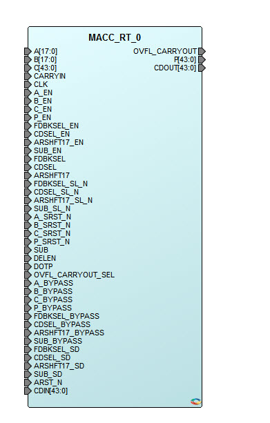
| Port Name | Direction | Type | Polarity | Description |
|---|---|---|---|---|
| DOTP | Input | Static | High | Dot-product mode. When DOTP = 1, MACC_RT block performs Dot-product of two pairs of 9-bit operands. When DOTP = 0, it is called the normal mode. |
| OVFL_CARRYOUT_SEL | Input | Static | High | Generate OVERFLOW or CARRYOUT with result
P. OVERFLOW when OVFL_CARRYOUT_SEL = 0 CARRYOUT when OVFL_CARRYOUT_SEL = 1 |
| DELEN | Input | Static | High | Enable Single-event Transient mitigation |
| CLK | Input | Dynamic | Rising edge | Input clocks. CLK is the clock for A[17:0], B[17:0], C[43:0], P[43:0], OVFL_CARRYOUT, ARSHFT17, CDSEL, FDBKSEL and SUB registers. |
| ARST_N | Input | Dynamic | Low | Asynchronous reset for all registers |
| A[17:0] | Input | Dynamic | High | Input data A. |
| A_BYPASS | Input | Static | High | Bypass data A registers. Connect to 1, if not registered. |
| A_SRST_N | Input | Dynamic | Low | Synchronous reset for data A registers. Connect to 1, if not registered. |
| A_EN | Input | Dynamic | High | Enable for data A registers. Connect to 1, if not registered. |
| B[17:0] | Input | Dynamic | High | Input data B. |
| B_BYPASS | Input | Static | High | Bypass data B registers. Connect to 1, if not registered. |
| B_SRST_N | Input | Dynamic | Low | Synchronous reset for data B registers. Connect to 1, if not registered. |
| B_EN | Input | Dynamic | High | Enable for data B registers. Connect to 1, if not registered. |
| P[43:0] | Output | — | High | Result data. Normal mode P = D + (CARRYIN + C) + (A * B), when SUB = 0 P = D + (CARRYIN + C) - (A * B), when SUB = 1 Dot-product mode P = D + (CARRYIN + C) + 512 * ((AL * BH) + (AH * BL)), when SUB = 0 P = D + (CARRYIN + C) - 512 * ((AL * BH) + (AH * BL)), when SUB = 1 Notation: AL = A[8:0], AH = A[17:9] BL = B[8:0], BH = B[17:9] Refer to Table 5-4 to see how operand D is obtained from P, CDIN or 0. |
| OVFL_CARRYOUT | Output | High | Overflow or CarryOut Refer to Table 5-5. |
|
| P_BYPASS | Input | Static | High | Bypass P and OVFL_CARRYOUT registers. Connect to 1, if not registered. |
| P_SRST_N | Input | Dynamic | Low | Synchronous reset for P and OVFL_CARRYOUT
registers. Connect to 1, if not registered. |
| P_EN | Input | Dynamic | High | Enable for P and OVFL_CARRYOUT registers. Connect to 1, if not registered. |
| CDOUT[43:0] | Output | Cascade | High | Cascade output of result P. CDOUT is the same as P. The entire bus must either be dangling or drive an entire CDIN of another MACC_RT block in cascaded mode. |
| CARRYIN | Input | Dynamic | High | CarryIn for operand C. |
| C[43:0] | Input | Dynamic | High | Routed input for operand C. In Dot-product mode, connect C[8:0] to the CARRYIN. |
| C_BYPASS | Input | Static | High | Bypass CARRYIN and C registers. Connect to 1, if not registered. |
| C_SRST_N | Input | Dynamic | Low | Synchronous reset for CARRYIN and C
registers. Connect to 1, if not registered. |
| C_EN | Input | Dynamic | High | Enable for CARRYIN and C registers. Connect to 1, if not registered. |
| CDIN[43:0] | Input | Cascade | High | Cascaded input for operand D. The entire bus must be driven by an entire CDOUT of another MACC_RT block. In Dot-product mode the CDOUT must also be generated by a MACC_RT block in Dot-product mode. Refer to Table 5-4 to see how CDIN is propagated to operand D. |
| ARSHFT17 | Input | Dynamic | High | Arithmetic right-shift for operand D. When asserted, a 17-bit arithmetic right-shift is performed on operand D going into the accumulator. Refer to Table 5-4 to see how operand D is obtained from P, CDIN or 0. |
| ARSHFT17_BYPASS | Input | Static | High | Bypass ARSHFT17 register. Connect to 1, if not registered. |
| ARSHFT17_SL_N | Input | Dynamic | Low | Synchronous load for ARSHFT17 register. Connect to 1, if not registered. See Table 5-7. |
| ARSHFT17_SD | Input | Static | High | Synchronous load data for ARSHFT17 register. See Table 5-7. |
| ARSHFT17_EN | Input | Dynamic | High | Enable for ARSHFT17 register. Connect to 1, if not registered. See Table 5-7. |
| CDSEL | Input | Dynamic | High | Select CDIN for operand D. When CDSEL = 1, propagate CDIN. When CDSEL = 0, propagate 0 or P depending on FDBKSEL. Refer to Table 5-4 to see how operand D is obtained from P, CDIN or 0. |
| CDSEL_BYPASS | Input | Static | High | Bypass CDSEL register. Connect to 1, if not registered. |
| CDSEL_SL_N | Input | Dynamic | Low | Synchronous load for CDSEL register. Connect to 1, if not registered. See Table 5-7. |
| CDSEL_SD | Input | Static | High | Synchronous load data for CDSEL register. See Table 5-7. |
| CDSEL_EN | Input | Dynamic | High | Enable for CDSEL register. Connect to 1, if not registered. See Table 5-7. |
| FDBKSEL | Input | Dynamic | High | Select the feedback from P for operand D. When FDBKSEL = 1, propagate the current value of result P register. Ensure P_BYPASS = 0 and CDSEL = 0. When FDBKSEL = 0, propagate 0. Ensure CDSEL = 0. Refer to Table 5-4 to see how operand D is obtained from P, CDIN or 0. |
| FDBKSEL_BYPASS | Input | Static | High | Bypass FDBKSEL register. Connect to 1, if not registered. |
| FDBKSEL_SL_N | Input | Dynamic | Low | Synchronous load for FDBKSEL register. Connect to 1, if not registered. See Table 5-7. |
| FDBKSEL_SD | Input | Static | High | Synchronous load data for FDBKSEL register. See Table 5-7. |
| FDBKSEL_EN | Input | Dynamic | High | Enable for FDBKSEL register. Connect to 1, if not registered. See Table 5-7. |
| SUB | Input | Dynamic | High | Subtract operation. |
| SUB_BYPASS | Input | Static | High | Bypass SUB register. Connect to 1, if not registered. |
| SUB_SL_N | Input | Dynamic | Low | Synchronous load for SUB register. Connect to 1, if not registered. See Table 5-7. |
| SUB_SD | Input | Static | High | Synchronous load data for SUB register. See Table 5-7. |
| SUB_EN | Input | Dynamic | High | Enable for SUB register. Connect to 1, if not registered. See Table 5-7. |
| ARST_N | _BYPASS | _CLK | _EN | _SL_N | _SD | D | Qn+1 |
|---|---|---|---|---|---|---|---|
| 0 | X | X | X | X | X | X | 0 |
| 1 | 0 | Not rising | X | X | X | X | Qn |
| 1 | 0 | — | 0 | X | X | X | Qn |
| 1 | 0 | — | 1 | 0 | SDn | X | SDn |
| 1 | 0 | — | 1 | 1 | X | D | D |
| 1 | 1 | X | 0 | X | X | X | Qn |
| 1 | 1 | X | 1 | 0 | SDn | X | SDn |
| 1 | 1 | X | 1 | 1 | X | D | D |