
16.3.4 SRAM
(Ask a Question)16.3.4.1 RAM1K18_RT
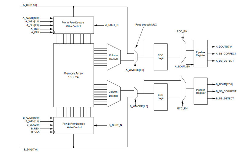
(Ask a Question)The RAM1K18_RT block contains 24,576 (18,432 with ECC) memory bits and is a true dual-port memory with two independent data ports A and B. The RAM1K18_RT memory can also be configured in two-port mode. All read/write operations to the RAM1K18_RT memory are synchronous. To improve the read-data delay, an optional pipeline register at the output is available. RAM1K18_RT also adds a Read-enable control to both dual-port and two-port modes. The RAM1K18_RT memory has two data ports which can be independently configured in any combination as follows.
- ECC Dual-Port RAM with the following configuration:
- 1Kx18 on both ports
- Non-ECC Dual-Port RAM with the following configurations:
- 1Kx18 on both ports
- 2Kx12 or 2Kx9 on both ports, but port B is read-only
- 2Kx9 on port A, 1Kx18 on port B
- ECC Two-Port RAM with the following configurations:
- Any of 512x36 or 1Kx18 on each port
- Non-ECC Two-Port RAM with port A write, port B read:
- Any of 1Kx18 or 2Kx9 on each port
- 2Kx12 on both ports
- Non-ECC Two-Port RAM with port A read, port B write:
- Any of 512x36, 1Kx18, or 2Kx9 on each port
FUNCTIONALITY
- Any of 512x36, 1Kx18, or 2Kx9 on each port
The main features of the RAM1K18_RT memory block are as follows:
- The address, data, block-port select, write enable and read-enable inputs are registered.
- An optional pipeline register with a separate enable and synchronous-reset is available at the read-data port to improve the clock-to-out delay.
- The registers in RAM1K18_RT block have an option to mitigate Single-event transients.
- There is an independent clock for each port. The memory will be triggered at the rising edge of the clock.
- Read from both ports at the same location is allowed.
- Read and write on the same location at the same time results in unknown data to be read. There is no collision prevention or detection. However, correct data are expected to be written into the memory.
- When ECC is enabled, each port of the RAM1K18_RT memory can raise flags to indicate single-bit-correct and double-bit-detect.
The following figure shows a simplified block diagram of the RAM1K18_RT memory block and the following table gives the port descriptions. The simplified block illustrates the two independent data ports and the read-data pipeline registers.
| Pin Name | Pin Direction | Type | Description | Polarity |
|---|---|---|---|---|
| A_ADDR[10:0] | Input | Dynamic | Port A address | — |
| A_BLK[2:0] | Input | Dynamic | Port A block selects | High |
| A_CLK | Input | Dynamic | Port A clock | Rising |
| A_DIN[17:0] | Input | Dynamic | Port A write-data | — |
| A_DOUT[17:0] | Output | Dynamic | Port A read-data | — |
| A_WEN[1:0] | Input | Dynamic | Port A write-enables (per byte) | High |
| A_REN | Input | Dynamic | Port A read-enable | High |
| A_WIDTH[1:0] | Input | Static | Port A width/depth mode select | — |
| A_DOUT_BYPASS | Input | Static | Port A pipeline register select | Low |
| A_WMODE[1:0] | Input | Static | Port A write mode | High |
| A_DOUT_EN | Input | Dynamic | Port A pipeline register enable | High |
| A_DOUT_SRST_N | Input | Dynamic | Port A pipeline register synchronous-reset | Low |
| B_ADDR[10:0] | Input | Dynamic | Port B address | — |
| B_BLK[2:0] | Input | Dynamic | Port B block selects | High |
| B_CLK | Input | Dynamic | Port B clock | Rising |
| B_DIN[17:0] | Input | Dynamic | Port B write-data | — |
| B_DOUT[17:0] | Output | Dynamic | Port B read-data | — |
| B_WEN[1:0] | Input | Dynamic | Port B write-enables (per byte) | High |
| B_REN | Input | Dynamic | Port B read-enable | High |
| B_WIDTH[1:0] | Input | Static | Port B width/depth mode select | — |
| B_WMODE[1:0] | Input | Static | Port B write mode | High |
| B_DOUT_BYPASS | Input | Static | Port B pipeline register select | Low |
| B_DOUT_EN | Input | Dynamic | Port B pipeline register enable | High |
| B_DOUT_SRST_N | Input | Dynamic | Port B pipeline register synchronous-reset | Low |
| ARST_N | Input | Global | Pipeline registers asynchronous-reset | Low |
| ECC | Input | Static | Enable ECC | High |
| ECC_DOUT_BYPASS | Input | Static | ECC pipeline register select | Low |
| A_SB_CORRECT | Output | Dynamic | Port A single-bit correct flag | High |
| A_DB_DETECT | Output | Dynamic | Port A double-bit detect flag | High |
| B_SB_CORRECT | Output | Dynamic | Port B single-bit correct flag | High |
| B_DB_DETECT | Output | Dynamic | Port B double-bit detect flag | High |
| DELEN | Input | Static | Enable SET mitigation | High |
| SECURITY | Input | Static | Lock access to SII | High |
| BUSY | Output | Dynamic | Busy signal from SII | High |
Port Description
A_WIDTH AND B_WIDTH
The following table lists the width/depth mode selections for each port. Two-port mode is in effect when the width of at least one port is 36, and A_WIDTH indicates the read width while B_WIDTH indicates the write width.
| Depth x Width | A_WIDTH/B_WIDTH |
|---|---|
| 2Kx9, 2Kx12 | 00 |
| 1Kx18 | 01 |
| 512x36 (Two-port) | 10 |
A_WEN AND B_WEN
The following table lists the write/read control signals for each port. Two-port mode is in effect when the width of at least one port is 36, and read operation is always enabled.
| Depth x Width | A_WEN/B_WEN | Result |
|---|---|---|
| 2Kx9, 2Kx12, 1Kx18 | 00 | Perform a read operation |
| 2Kx9, 2Kx12 | 11 | Perform a write operation |
| 1Kx18 | 01 | Write [8:0] |
| 10 | Write [17:9] | |
| 11 | Write [17:0] | |
| 512x36 (Two-port write) | B_WEN[0] = 1 | Write B_DIN[8:0] |
| B_WEN[1] = 1 | Write B_DIN[17:9] | |
| A_WEN[0] = 1 | Write A_DIN[8:0] | |
| A_WEN[1] = 1 | Write A_DIN[17:9] |
A_ADDR AND B_ADDR
The following table lists the address buses for the two ports. 11 bits are needed to address the 2K independent locations in x9 mode. In wider modes, fewer address bits are used. The required bits are MSB justified and unused LSB bits must be tied to 0. A_ADDR is synchronized by A_CLK while B_ADDR is synchronized to B_CLK. Two-port mode is in effect when the width of at least one port is 36, and A_ADDR provides the read-address while B_ADDR provides the write-address.
| Depth x Width | A_ADDR/B_ADDR | |
|---|---|---|
| Used Bits | Unused Bits (must be tied to 0) | |
| 2Kx9, 2Kx12 | [10:0] | None |
| 1Kx18 | [10:1] | [0] |
| 512x36 (Two-port) | [10:2] | [1:0] |
A_DIN AND B_DIN
The following table lists the data input buses for the two ports. The required bits are LSB justified and unused MSB bits must be tied to 0. Two-port mode is in effect when the width of at least one port is 36, and A_DIN provides the MSB of the write-data while B_DIN provides the LSB of the write-data.
| Depth x Width | A_DIN/B_DIN | |
|---|---|---|
| Used Bits | Unused Bits (must be tied to 0) | |
| 2Kx9 | [8:0] | [17:9] |
| 2Kx12 | [11:0] | [17:12] |
| 1Kx18 | [17:0] | None |
| 512x36 (Two-port write) | A_DIN[17:0] is [35:18] B_DIN[17:0] is [17:0 ] | None |
A_DOUT AND B_DOUT
The following table lists the data output buses for the two ports. The required bits are LSB justified. Two-port mode is in effect when the width of at least one port is 36, and A_DOUT provides the MSB of the read-data while B_DOUT provides the LSB of the read-data.
| Depth x Width | A_DOUT/B_DOUT | |
|---|---|---|
| Used Bits | Unused Bits | |
| 2Kx9 | [8:0] | [17:9] |
| 2Kx12 | [11:0] | [17:12] |
| 1Kx18 | [17:0] | None |
| 512x36 (Two-port read) | A_DOUT[17:0] is [35:18] B_DOUT[17:0] is [17:0 ] | None |
A_BLK AND B_BLK
The following table lists the block-port select control signals for the two ports. A_BLK is synchronized by A_CLK while B_BLK is synchronized to B_CLK. Two-port mode is in effect when the width of at least one port is 36, and A_BLK controls the read operation while B_BLK controls the write operation.
| Block-port Select Signal | Value | Result |
|---|---|---|
| A_BLK[2:0] | 111 | Perform read or write operation on Port A. In 36 width mode, perform a read operation from both ports A and B. |
| A_BLK[2:0] | Any one bit is 0 | No operation in memory from Port A. Port A read-data will be forced to 0. In 36 width mode, the read-data from both ports A and B will be forced to 0. |
| B_BLK[2:0] | 111 | Perform read or write operation on Port B. In 36 width mode, perform a write operation to both ports A and B. |
| B_BLK[2:0] | Any one bit is 0 | No operation in memory from Port B. Port B read-data will be forced to 0, unless it is a 36 width mode and write operation to both ports A and B is gated. |
A_WMODE AND B_WMODE
Specifies the write mode for each port:
- Logic 00 = Read-data port holds the previous value.
- Logic X1 = This setting is invalid.
- Logic 10 = This setting is invalid.
A_CLK AND B_CLK
All signals in ports A and B are synchronous to the corresponding port clock. All addresses, data, block-port select, write enable, and read-enable inputs must be setup before the rising edge of the clock. The read or write operation begins with the rising edge. Two-port mode is in effect when the width of at least one port is 36, and A_CLK provides the read clock while B_CLK provides the write clock.
A_REN AND B_REN
Enables read operation from the memory on the corresponding port.
Read-data Pipeline Register Control signals
- A_DOUT_BYPASS and B_DOUT_BYPASS
- A_DOUT_EN and B_DOUT_EN
- A_DOUT_SRST_N and B_DOUT_SRST_N
Two-port mode is in effect when the width of at least one port is 36, and the A_DOUT register signals control the MSB of the read-data while the B_DOUT register signals control the LSB of the read-data.
The following table describes the functionality of the control signals on the A_DOUT and B_DOUT pipeline registers.
| ARST_N | _BYPASS | _CLK | _EN | _SRST_N | D | Qn+1 |
|---|---|---|---|---|---|---|
| 0 | X | X | X | X | X | 0 |
| 1 | 0 | Not rising | X | X | X | Qn |
| 1 | 0 | ↑ | 0 | X | X | Qn |
| 1 | 0 | ↑ | 1 | 0 | X | 0 |
| 1 | 0 | ↑ | 1 | 1 | D | D |
| 1 | 1 | X | X | X | D | D |
ARST_N
Connects the Read-data pipeline registers to the global Asynchronous-reset signal.
ECC AND ECC_DOUT_BYPASS
Controls ECC operation.
- ECC = 0: Disable ECC.
- ECC = 1, ECC_DOUT_BYPASS = 0: Enable ECC Pipelined.
- ECC Pipelined mode inserts an additional clock cycle to Read-data.
- ECC = 1, ECC_DOUT_BYPASS = 1: Enable ECC Non-pipelined.
A_SB_CORRECT AND B_SB_CORRECT
- ECC = 1, ECC_DOUT_BYPASS = 1: Enable ECC Non-pipelined.
Output flag indicates single-bit correction was performed on the corresponding port.
A_DB_DETECT AND B_DB_DETECT
Output flag indicates double-bit detection was performed on the corresponding port.
DELEN
Enable Single-event Transient mitigation.
SECURITY
Controls signal, when 1 locks the entire RAM1K18_RT memory from being accessed by the SII.
BUSY
This output indicates that the RAM1K18_RT memory is being accessed by the SII.
16.3.4.2 RAM64x18_RT
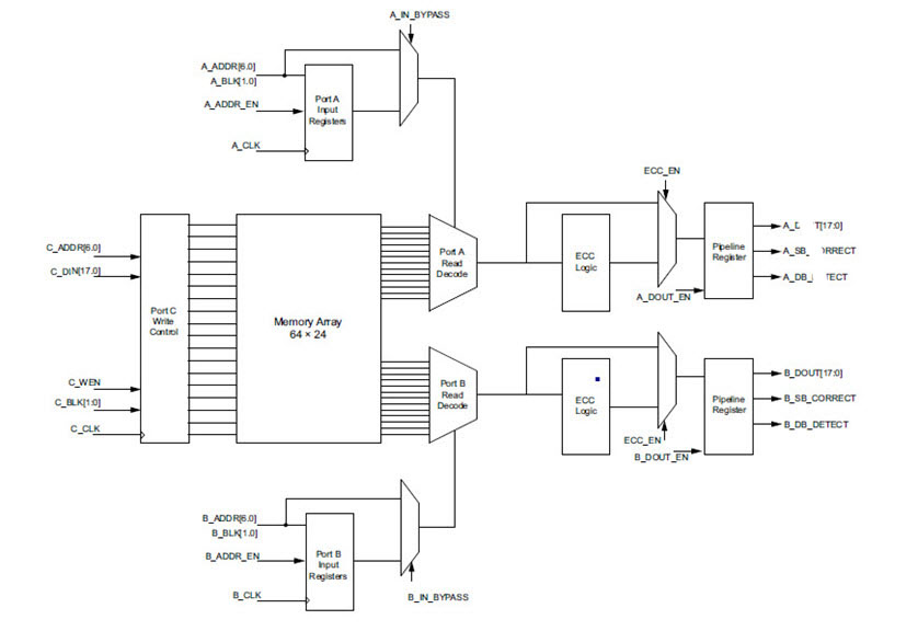
(Ask a Question)The RAM64x18_RT block contains 1,536 (1,152 with ECC) memory bits and is a three-port memory providing one write port and two read ports. Write operations to the RAM64x18_RT memory are synchronous. Read operations can be asynchronous or synchronous for setting up the address and reading out the data. Enabling synchronous operation at the read-address port improves setup timing for the read-address and its enable signals. Enabling synchronous operation at the read-data port improves clock-to-out delay. Each data port on the RAM64x18_RT memory can be independently configured in any combination as follows.
- ECC Three-Port RAM with the following configuration:
- 64x18 on all three ports
- Non-ECC Three-Port RAM with the following configurations:
- Any of 64x18 or 128x9 on each port
- 128x12 on all three ports
FUNCTIONALITY
The main features of the RAM64x18_RT memory block are as follows.
- There are two independent read-data ports A and B, and one write-data port C.
- The write operation is always synchronous. The write-address, write-data, C block-port select and write enable inputs are registered.
- For both read-data ports, setting up the address can be synchronous or asynchronous.
- The two read-data ports have address registers with a separate enable and synchronous-reset for synchronous mode operation, which can also be bypassed for asynchronous mode operation.
- The two read-data ports have output registers with a separate enable and synchronous-reset for pipeline mode operation, which can also be bypassed for asynchronous mode operation.
- Therefore, there are four read operation modes for ports A and B:
- Synchronous read-address without read-data pipeline registers (sync-async)
- Synchronous read-address with read-data pipeline registers (sync-sync)
- Asynchronous read-address without read-data pipeline registers (async-async)
- Asynchronous read-address with read-data pipeline registers (async-sync)
- In ECC mode, all ports have word widths equal to 18 bits.
- In non-ECC mode, each port can be independently configured to any of the following depth/width: 64x18 or 128x9. In addition, all the ports can be configured to 128x12.
- The registers in RAM64x18_RT block have an option to mitigate Single-event transients.
- There is an independent clock for each port. The memory will be triggered at the rising edge of the clock.
- Read from both ports A and B at the same location is allowed.
- Read and write on the same location at the same time results in unknown data to be read.
- There is no collision prevention or detection. However, correct data are expected to be written into the memory.
- When ECC is enabled, each port of the RAM64x18_RT memory can raise flags to indicate single-bit-correct and double-bit-detect.
The following figure shows a simplified block diagram of the RAM64x18_RT memory block and the following table gives the port descriptions. The simplified block illustrates the three independent read/write ports and the pipeline registers on the read port.
| Pin Name | Pin Direction | Type | Description | Polarity | |||
|---|---|---|---|---|---|---|---|
| A_ADDR[6:0] | Input | Dynamic | Port A read-address | — | |||
| A_BLK[1:0] | Input | Dynamic | Port A block selects | High | |||
| A_WIDTH | Input | Static | Port A width/depth mode selection | — | |||
| A_DOUT[17:0] | Output | Dynamic | Port A read-data | — | |||
| A_DOUT_EN | Input | Dynamic | Port A read-data pipeline register enable | High | |||
| A_DOUT_BYPASS | Input | Static | Port A read-data pipeline register select | Low | |||
| A_DOUT_SRST_N | Input | Dynamic | Port A read-data pipeline register synchronous-reset | Low | |||
| A_CLK | Input | Dynamic | Port A registers clock | Rising | |||
| A_ADDR_EN | Input | Dynamic | Port A read-address register enable | High | |||
| A_ADDR_BYPASS | Input | Static | Port A read-address register select | Low | |||
| A_ADDR_SRST_N | Input | Dynamic | Port A read-address register synchronous-reset | Low | |||
| B_ADDR[6:0] | Input | Dynamic | Port B read-address | — | |||
| B_BLK[1:0] | Input | Dynamic | Port B block selects | High | |||
| B_WIDTH | Input | Static | Port B width/depth mode selection | — | |||
| B_DOUT[17:0] | Output | Dynamic | Port B read-data | — | |||
| B_DOUT_EN | Input | Dynamic | Port B read-data pipeline register enable | High | |||
| B_DOUT_BYPASS | Input | Static | Port B read-data pipeline register select | Low | |||
| B_DOUT_SRST_N | Input | Dynamic | Port B read-data pipeline register synchronous-reset | Low | |||
| B_CLK | Input | Dynamic | Port B registers clock | Rising | |||
| B_ADDR_EN | Input | Dynamic | Port B read-address register enable | High | |||
| B_ADDR_BYPASS | Input | Static | Port B read-address register select | Low | |||
| B_ADDR_SRST_N | Input | Dynamic | Port B read-address register synchronous-reset | Low | |||
| C_ADDR[6:0] | Input | Dynamic | Port C address | — | |||
| C_CLK | Input | Dynamic | Port C clock | Rising | |||
| C_DIN[17:0] | Input | Dynamic | Port C write-data | — | |||
| C_WEN | Input | Dynamic | Port C write enable | High | |||
| C_BLK[1:0] | Input | Dynamic | Port C block selects | High | |||
| C_WIDTH | Input | Static | Port C width/depth mode selection | — | |||
| ARST_N | Input | Global | Read-address and Read-data pipeline registers asynchronous-reset | Low | |||
| ECC | Input | Static | Enable ECC | High | |||
| ECC_DOUT_BYPASS | Input | Static | ECC pipeline register select | Low | |||
| A_SB_CORRECT | Output | Dynamic | Port A single-bit correct flag | High | |||
| A_DB_DETECT | Output | Dynamic | Port A double-bit detect flag | High | |||
| B_SB_CORRECT | Output | Dynamic | Port B single-bit correct flag | High | |||
| B_DB_DETECT | Output | Dynamic | Port B double-bit detect flag | High | |||
| DELEN | Input | Static | Enable SET mitigation | High | |||
| SECURITY | Input | Static | Lock access to SII | High | |||
| BUSY | Output | Dynamic | Busy signal from SII | High | |||
PORT DESCRIPTION
A_WIDTH, B_WIDTH AND C_WIDTH
The following table lists the width/depth mode selections for each port.
| Depth x Width | A_WIDTH/B_WIDTH/C_WIDTH |
|---|---|
| 128x9, 128x12 | 0 |
| 64x16, 64x18 | 1 |
C_WEN
This is the write enable signal for port C.
A_ADDR, B_ADDR AND C_ADDR
The following table lists the address buses for each port. 7 bits are required to address 128 independent locations in x9 mode. In wider modes, fewer address bits are used. The required bits are MSB justified and unused LSB bits must be tied to 0.
| Depth x Width | A_ADDR/B_ADDR/C_ADDR | |
|---|---|---|
| Used Bits | Unused Bits (must be tied to zero) | |
| 128x9, 128x12 | [6:0] | None |
| 64x18 | [6:1] | [0] |
C_DIN
The following table lists the write-data input for port C. The required bits are LSB justified and unused MSB bits must be tied to 0.
| Depth x Width | C_DIN | |
|---|---|---|
| Used Bits | Unused Bits (must be tied to 0) | |
| 128x9 | [8:0] | [17:9] |
| 128x12 | [11:0] | [17:12] |
| 64x18 | [17:0] | None |
A_DOUT AND B_DOUT
The following table lists the read-data output buses for ports A and B. The required bits are LSB justified.
| Depth x Width | A_DOUT/B_DOUT | |
|---|---|---|
| Used Bits | Unused Bits | |
| 128x9 | [8:0] | [17:9] |
| 128x12 | [11:0] | [17:12] |
| 64x18 | [17:0] | None |
A_BLK, B_BLK AND C_BLK
The following table lists the block-port select control signals for the ports.
| Block-port Select Signal | Value | Result |
|---|---|---|
| A_BLK[1:0] | Any one bit is 0 | Port A is not selected and its read-data will be forced to zero. |
| 11 | Perform read operation from port A. | |
| B_BLK[1:0] | Any one bit is 0 | Port B is not selected and its read-data will be forced to zero. |
| 11 | Perform read operation from port B. | |
| C_BLK[1:0] | Any one bit is 0 | Port C is not selected. |
| 11 | Perform write operation to port C. |
C_CLK
All signals on port C are synchronous to this clock signal. All write-address, write-data, C block-port select and write-enable inputs must be set up before the rising edge of the clock. The write operation begins with the rising edge.
Read-address and Read-data Pipeline Register Control signals
- A_DOUT_BYPASS, A_ADDR_BYPASS, B_DOUT_BYPASS, and B_ADDR_BYPASS
- A_DOUT_EN, A_ADDR_EN, B_DOUT_EN, and B_ADDR_EN
- A_DOUT_SRST_N, A_ADDR_SRST_N, B_DOUT_SRST_N, and B_ADDR_SRST_N
The following table describes the functionality of the control signals on the A_ADDR, B_ADDR, A_DOUT, and B_DOUT registers.
| ARST_N | _BYPASS | _CLK | _EN | _SRST_N | D | Qn+1 |
|---|---|---|---|---|---|---|
| 0 | X | X | X | X | X | 0 |
| 1 | 0 | Not rising | X | X | X | Qn |
| 1 | 0 | ↑ | 0 | X | X | Qn |
| 1 | 0 | ↑ | 1 | 0 | X | 0 |
| 1 | 0 | ↑ | 1 | 1 | D | D |
| 1 | 1 | X | X | X | D | D |
ARST_N
Connects the read-address and read-data pipeline registers to the global Asynchronous-reset signal.
ECC and ECC_DOUT_BYPASS
Controls ECC operation.
- ECC = 0: Disable ECC.
- ECC = 1, ECC_DOUT_BYPASS = 0: Enable ECC Pipelined.
- ECC Pipelined mode inserts an additional clock cycle to Read-data.
- ECC = 1, ECC_DOUT_BYPASS = 1: Enable ECC Non-pipelined.
A_SB_CORRECT AND B_SB_CORRECT
Output flag indicates single-bit correction was performed on the corresponding port.
A_DB_DETECT and B_DB_DETECT
Output flag indicates double-bit detection was performed on the corresponding port.
DELEN
Enable Single-event Transient mitigation.
SECURITY
Control signal, when 1 locks the entire RAM64x18_RT memory from being accessed by the SII.
BUSY
This output indicates that the RAM64x18_RT memory is being accessed by the SII.