
45.10.4 Analog-to-Digital Converter (ADC) Characteristics
| Symbol | Parameters | Conditions | Min. | Typ. | Max. | Unit |
|---|---|---|---|---|---|---|
| Res | Resolution | - | - | 12 | bits | |
| Rs | Sampling rate(2) | SAMPLEN = 3 resolution 12 bit (CTRLC.RESSEL= 0) |
10 | - | 1000 | ksps |
| Nb_cycles | Differential mode Number of ADC clock cycles SAMPCTRL.OFFCOMP=1 | resolution 12 bit (CTRLC.RESSEL= 0) |
- | 16 | - | cycles |
| resolution 10 bit (CTRLC.RESSEL= 2) |
14 | |||||
| resolution 8 bit (CTRLC.RESSEL= 3) |
12 | |||||
| Differential mode Number of ADC clock cycles SAMPCTRL.OFFCOMP=0 SAMPLEN corresponds to the decimal value of SAMPCTRL.SAMPLEN[5:0] register | resolution 12 bit (CTRLC.RESSEL= 0) |
- | SAMPLEN+13 | - | cycles | |
| resolution 10 bit (CTRLC.RESSEL= 2) |
SAMPLEN+11 | |||||
| resolution 8 bit (CTRLC.RESSEL= 3) |
SAMPLEN+9 | |||||
| Single-ended mode Number of ADC clock cycles SAMPCTRL.OFFCOMP=1 | resolution 12 bit (CTRLC.RESSEL= 0) |
- | 16 | - | cycles | |
| resolution 10 bit (CTRLC.RESSEL= 2) |
15 | |||||
| resolution 8 bit (CTRLC.RESSEL= 3) |
13 | |||||
| Single-ended mode Number of ADC clock cycles SAMPCTRL.OFFCOMP=0 SAMPLEN corresponds to the decimal value of SAMPCTRL.SAMPLEN[5:0] register | resolution 12 bit (CTRLC.RESSEL= 0) |
- | SAMPLEN+13 | - | cycles | |
| resolution 10 bit (CTRLC.RESSEL= 2) |
SAMPLEN+12 | |||||
| resolution 8 bit (CTRLC.RESSEL= 3) |
SAMPLEN+10 | |||||
| fadc | ADC Clock frequency | - | 160 | - | 16000 | kHz |
| Ts | Sampling time | SAMPCTRL.OFFCOMP = 1 | 250 | - | 25000 | ns |
| SAMPCTRL.OFFCOMP = 0 | (SAMPLEN+1)/fadc | - | - | s | ||
| Sampling time with INTREF as input | 10 | - | - | us | ||
| VCNV | Conversion range | Differential mode | -VREF | - | +VREF | V |
| Conversion range | Single-ended mode | 0 | - | VREF | ||
| Vref | Reference input | - | 2 | - | VDDANA-0.6 | V |
| Vin | Input channel range | - | 0 | - | VDDANA | V |
| Vcmin | Input common mode voltage | CTRLC.R2R = 1 | 0.2 | - | VREF-0.2 | V |
| CTRLC.R2R = 0 | VREF/2-0.2 | - | VREF/2+0.2 | V | ||
| CSAMPLE | Input sampling capacitance | - | - | 3.2 | pF | |
| RSAMPLE | Input sampling on-resistance | For a sampling rate at 1 Msps | - | 1000 | 1715 | Ω |
| Rref | Reference input source resistance | 0 | - | 1000 | kΩ |
Note:
- These values are based on simulation and not covered by test limits in production or characterization.
- Sampling rate (in samples per second) is equal to (fadc/Nb_cycles).
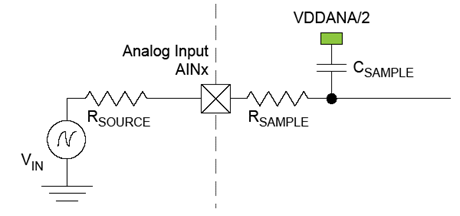
The minimum sampling time tsamplehold for a given Rsource can be calculated using this formula:
For 12-bit accuracy:
| Symbol | Parameter | Conditions | Measurement | Unit | ||
|---|---|---|---|---|---|---|
| Min. | Typ | Max. | ||||
| ENOB | Effective Number of bits | Vddana = 5.0V Vref = Vddana | 10.5 | 10.8 | 11.3 | bits |
| Vddana = 2.7V Vref = 2.0V | 9.9 | 10.0 | 11.2 | |||
| TUE | Total Unadjusted Error Condition: R2R disabled with offset and gain compensation (REFCOMP = 1 and OFFCOMP = 1) |
Vddana = 5.0V Vref = Vddana | - | 4.2 | 6.7 | LSB |
| Vddana = 2.7V Vref = 2.0V | - | 4.8 | 7.9 | |||
| INL | Integral Non Linearity | Vddana = 5.0V Vref = Vddana | - | +/-1.5 | +/-3 | LSB |
| Vddana = 2.7V Vref = 2.0V | - | +/-3.2 | +/-3.9 | |||
| DNL | Differential Non Linearity | Vddana = 5.0V Vref = Vddana | - | -0.8/+1.1 | -1/+1.9 | LSB |
| Vddana = 2.7V Vref = 2.0V | - | -0.9/+1.3 | -1/+2.1 | |||
| GE | Gain Error | Vddana = 2.7V Vref = 2.0V | - | +/-18 | +/-57 | mV |
| Vddana = 5.0V Vref = 4.096V | - | +/-41 | +/-100 | |||
| Vddana = 3.0V Vref = Vddana | - | +/-17 | +/-66 | |||
| Vddana = 5.0V Vref = Vddana | - | +/-39 | +/-81 | |||
| TCg | Gain Drift | Vddana = 5.0V Vref = Vddana | -250 | -210 | -170 | uV/°C |
| OE | Offset Error | Vddana = 2.7V Vref = 2.0V | - | +/-1.4 | +/-11 | mV |
| Vddana = 5.0V Vref = 4.096V | - | +/-6 | +/-18 | |||
| Vddana = 3.0V Vref=Vddana | - | +/-2 | +/-9 | |||
| Vddana = 5.0V Vre f= Vddana | - | +/-0.2 | +/-23 | |||
| Tco | Offset Drift | Vddana = 5.0V Vref = Vddana | 20 | 80 | 120 | uV/°C |
| SFDR | Spurious Free Dynamic Range | Fs = 1Msps / Fin = 14 kHz / Full range Input signal Vddana = 5.0V Vref = Vddana | 71 | 75 | 81 | dB |
| SINAD | Signal to Noise and Distortion ratio | 65 | 67 | 68 | ||
| SNR | Signal to Noise ratio | 67 | 68 | 69 | ||
| THD | -77 | -74 | -70 | |||
| Noise RMS | External Reference voltage | - | 0.5 | 2.0 | mV | |
Note:
- These values are based on characterization and not covered by test limits in production.
| Symbol | Parameter | Conditions | Measurement | Unit | ||
|---|---|---|---|---|---|---|
| Min. | Typ | Max. | ||||
| ENOB | Effective Number of bits | Vddana = 5.0V Vref=Vddana | 9.1 | 9.7 | 10 | bits |
| Vddana = 2.7V Vref=2.0V | 9.0 | 9.2 | 10 | |||
| TUE | Total Unadjusted
Error Condition: R2R disabled with offset and gain compensation (REFCOMP = 1 and OFFCOMP = 1) |
Vddana = 5.0V Vref = Vddana | - | 18.4 | 26.5 | LSB |
| Vddana = 2.7V Vref = 2.0V | - | 30.4 | 53.8 | |||
| INL | Integral Non Linearity | Vddana = 5.0V Vref = Vddana | - | +/-2.2 | +/-4 | LSB |
| Vddana = 2.7V Vref = 2.0V | - | +/-4.1 | +/-6 | |||
| DNL | Differential Non Linearity | Vddana = 5.0V Vref=Vddana | - | -0.8/+1 | -1/+1.9 | LSB |
| Vddana = 2.7V Vref = 2.0V | - | -1/+1.1 | -1/+2.4 | |||
| GE | Gain Error | Vddana = 2.7V Vref = 2.0V | - | +/-13 | +/-28 | mV |
| Vddana = 5.0V Vref = 4.096V | - | +/-26 | +/-52 | |||
| Vddana = 3.0V Vref = Vddana | - | +/-14 | +/-24 | |||
| Vddana = 5.0V Vref = Vddana | - | +/-22 | +/-42 | |||
| TCg | Gain Drift | Vddana = 5.0V Vref = Vddana | -170 | -140 | -80 | uV/°C |
| OE | Offset Error | Vddana = 2.7V Vref = 2.0V | - | +/-2.2 | +/-21 | mV |
| Vddana = 5.0V Vref = 4.096V | - | +/-2.3 | +/-61 | |||
| Vddana = 3.0V Vref=Vddana | - | +/-15 | +/-42 | |||
| Vddana = 5.0V Vref = Vddana | - | +/-31 | +/-80 | |||
| Tco | Offset Drift | Vddana = 5.0V Vref = Vddana | 160 | 180 | 210 | uV/°C |
| SFDR | Spurious Free Dynamic Range | Fs = 1Msps / Fin = 14 kHz / Full range Input signal Vddana = 5.0V Vref = Vddana | 69 | 71 | 73 | dB |
| SINAD | Signal to Noise and Distortion ratio | 57 | 60 | 61 | ||
| SNR | Signal to Noise ratio | 57 | 61 | 61 | ||
| THD | -72 | -70 | -66 | |||
| Noise RMS | External Reference voltage | - | 0.7 | 2.0 | mV | |
Note:
- These values are based on characterization and not covered by test limits in production.
| Symbol | Parameters | Conditions | Ta | Typ. | Max. | Units |
|---|---|---|---|---|---|---|
| IDD VDDANA | Differential mode | fs = 1Msps / Reference buffer disabled / BIASREFBUF = '110', BIASREFCOMP = '111' VDDANA=Vref= 5.5V | Max 85°C Typ 25°C | 905 | 1021 | uA |
| fs = 1Msps / Reference buffer enabled / BIASREFBUF = '110', BIASREFCOMP = '111' VDDANA = Vref = 5.5V | 1144 | 1403 | ||||
| fs = 10 ksps / Reference buffer disabled / BIASREFBUF = '110', BIASREFCOMP = '111' VDDANA=Vref= 5.5V | 381 | 460 | ||||
| fs = 10 ksps / Reference buffer enabled / BIASREFBUF = '110', BIASREFCOMP = '111' VDDANA = Vref = 5.5V | 609 | 857 | ||||
| Single Ended mode | fs = 1Msps / Reference buffer disabled / BIASREFBUF = '110', BIASREFCOMP = '111' VDDANA = Vref = 5.5V | Max 85°C Typ 25°C | 984 | 1077 | uA | |
| fs = 1Msps / Reference buffer enabled / BIASREFBUF = '110', BIASREFCOMP = '111' VDDANA = Vref=5.5V | 1178 | 1444 | ||||
| fs = 10 ksps / Reference buffer disabled / BIASREFBUF = '110', BIASREFCOMP = '111' VDDANA = Vref = 5.5V | 437 | 528 | ||||
| fs = 10 ksps / Reference buffer enabled / BIASREFBUF = '110', BIASREFCOMP = '111' VDDANA = Vref = 5.5V | 635 | 888 |
Note:
- These values are based on characterization.