
13.4.3 Primary Oscillator (POSC)
The dsPIC33AK512MPS512 devices contain one instance of the Primary Oscillator (POSC). The Primary Oscillator is available on the OSCO and OSCI pins of the dsPIC33A devices. This connection enables an external crystal (or ceramic resonator) to provide the clock to the device. The POSC oscillator is enabled by POSCEN bit in OSCCTRL register and is ready for operation when POSCRDY bit is set in OSCCTRL register. The Primary Oscillator has three modes of operation listed in Table 13-6.
| POSCMD[1:0] bits in OSCCFG register | Mode Description |
|---|---|
| 3 | POSC is disabled. OCSI can be used as regular I/O pins. The OSCO pin is controlled by the POSCIOFNC bit in the OSCCFG register. |
| 2-1 | Quartz Crystal Mode. OSCO and OSCI pins are connected to a crystal driver. |
| 0 | External Clock Mode (EC). The clock source must be connected to the OSCI pin. The OSCO pin is controlled by the POSCIOFNC bit in the OSCCFG register. |
If the Primary Oscillator is disabled or configured in EC mode, the OSCO pin can output the device system (CPU) clock when the POSCIOFNC bit in the OSCCFG register is set.
Figure 13-8 shows a recommended Pierce oscillator circuit diagram for the dsPIC33A devices.
Capacitors C1 and C2 form a load capacitance (CLOAD) for the crystal, and the R1 resistor limits the power dissipated in the quartz. The optimum load capacitance for a given crystal is specified by the crystal manufacturer. Load capacitance can be calculated as shown in Equation 13-2.
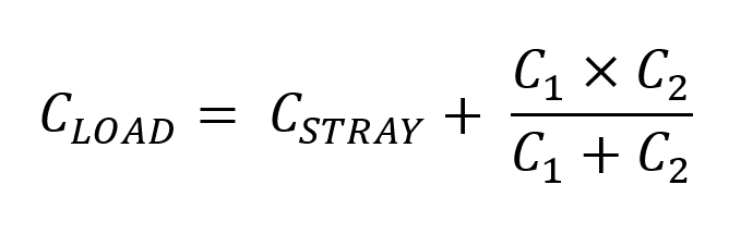
Where CSTRAY is the stray capacitance between the quartz crystal pads on the board (in many cases, it can be assumed 1-3 pF), C1 and C2 are capacitors connected to the crystal.
Assuming that C1 = C2, Equation 13-3 gives the capacitors C1 and C2 values for a given crystal load and stray capacitance.
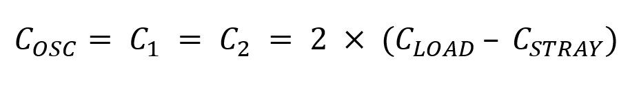
Where CLOAD is a nominal load capacitance from the crystal spec, and CSTRAY is the stray capacitance between the quartz crystal pads on the board.
If the power dissipated in the crystal is higher than the value specified by the crystal manufacturer, the current must be limited by resistor R1 to avoid overdriving the crystal. An initial estimation of R1 can be obtained by considering the voltage divider formed by R1 and C1. Thus, the initial value of R1 is equal to the impedance of C1 as shown in Equation 13-4.
Where F is the crystal nominal oscillation frequency.
The power dissipating in quartz can be verified with an oscilloscope using Equation 13-5.
Where RESR is the series resistance from the crystal specification, F is the crystal nominal oscillation frequency, CSTRAY is the stray capacitance between the quartz crystal pads on the board, CPROBE is the capacitance of the oscilloscope probe connected to C2 and Vpp is the peak-to-peak amplitude of the signal on the C2 capacitor measured with an oscilloscope.
The calculated power must be less than what is specified in the crystal specification.
The Primary Oscillator gain for the Crystal mode is selected by the GAIN[2:0] bits. For each gain mode, the GAIN[2:0] bits set the oscillator driver transconductance level as specified in the electrical specification.
The transconductance of the crystal oscillator driver, required to start the oscillation quickly enough and sustain stable oscillation, must be about four times greater than the transconductance of the quartz crystal circuit.
The transconductance of the quartz crystal circuit can be estimated by using Equation 13-6.
Where RESR is the equivalent series resistance from the crystal spec, R1 is a power-limiting resistor, F is the crystal nominal oscillation frequency, CSTRAY is the stray capacitance between the quartz crystal pads on the board, and COSC/2 is the external load capacitance for the crystal.
The transconductance selected by GAIN[2:0] bits should be at least four times larger than the calculated Gmin; however, gain settings that are too high may overload the crystal.